


Top Companies Shaping the Global Chiplet Industry
The top companies in the chiplet industry are profiled by core technologies, major products, packaging expertise, market trends, and regional presence.
Introduction
Overview of the Global Chiplet Industry
The global chiplet industry has moved from an experimental design method into a practical architecture for processors, artificial intelligence accelerators, networking devices, automotive controllers, and high-performance computing systems. A modern automobile can contain over 1,000 semiconductor devices, while a smartphone can integrate 160 chip functions, creating demand for architectures that combine specialized computing, memory, connectivity, security, and input-output functions efficiently. Chiplets address this complexity by dividing a large system-on-chip into smaller dies that can be designed, manufactured, tested, and upgraded independently before being assembled inside 1 package. This modular approach allows manufacturers to select different fabrication nodes for compute cores, cache, analog circuits, memory controllers, and communication interfaces.
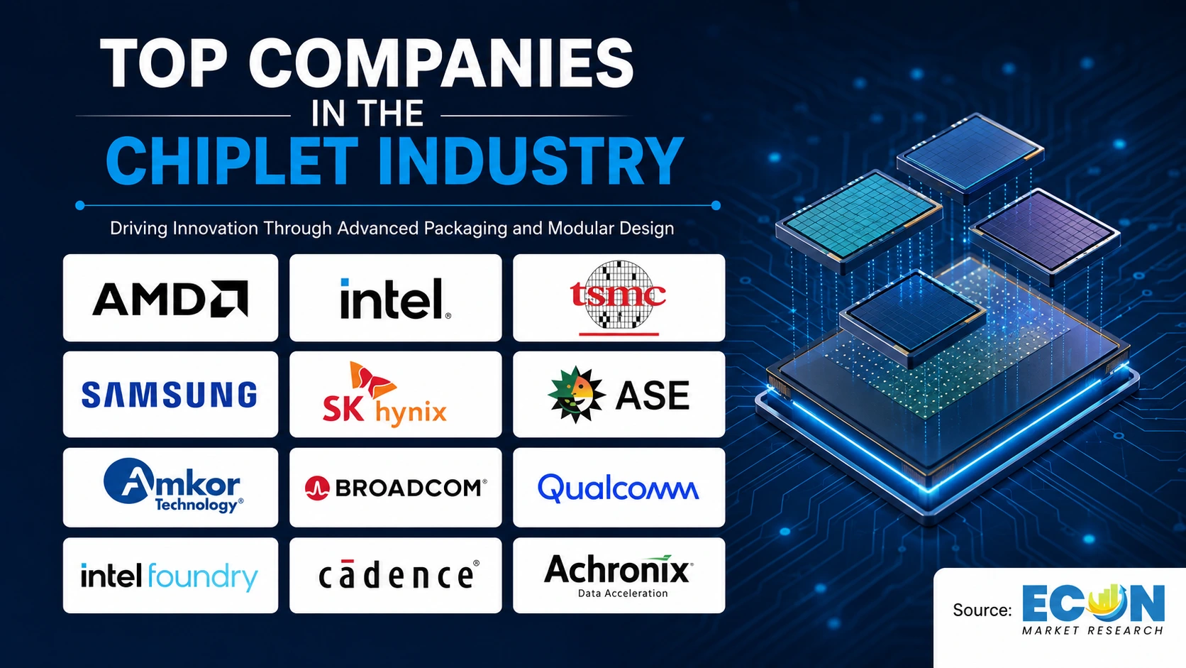
Commercial chiplet systems now operate across client computing, data centers, supercomputers, and generative AI infrastructure. Current server processor families support configurations reaching 192 CPU cores, while advanced packages integrate logic dies, high-bandwidth memory stacks, interposers, and active base dies through 2.5D and 3D assembly methods. The competitive structure includes processor designers, foundries, outsourced semiconductor assembly and test providers, substrate manufacturers, interface developers, electronic design automation specialists, and testing-equipment suppliers. Open specifications are also reducing dependence on proprietary die-to-die links, enabling a future in which qualified chiplets from different suppliers can communicate through standardized physical, protocol, test, and management layers.
Market Evolution and Growth Drivers
Chiplet adoption accelerated when semiconductor companies began separating high-performance compute dies from input-output functions that did not require the same manufacturing process. In 2019, the introduction of mainstream desktop processors based on the Zen 2 architecture demonstrated that 7-nanometer compute chiplets could be connected to a separate input-output die. That generation delivered a 15% instructions-per-clock improvement, while the following Zen 3 generation recorded a 19% improvement. The architecture demonstrated that modular dies could support consumer-scale production rather than remaining limited to research processors or specialized supercomputers.
Advanced packaging matured at the same time. Embedded bridge packaging entered mass production in 2017, while active-base-die stacking entered production in 2019. These technologies enabled shorter electrical paths, higher interconnect density, and better power efficiency than conventional printed-circuit-board connections. Growth is now driven by artificial intelligence models, cloud computing, automotive electronics, 5G infrastructure, scientific computing, and the rising cost of manufacturing very large monolithic dies. Chiplets allow stable interface, analog, and memory-controller components to remain on mature nodes while compute blocks move to newer nodes, extending reusable intellectual property across multiple product generations.
Top 5 Latest Trends in the Chiplet Industry
UCIe 3.0 and Open Die-to-Die Interoperability
2.5D and 3D Heterogeneous Integration
Chiplet-Based AI Accelerators with High-Bandwidth Memory
Process-Node Optimization and Reusable Silicon Blocks
Package-Level Testing, Thermal Management, and Telemetry
1. UCIe 3.0 and Open Die-to-Die Interoperability
The transition from proprietary interconnects to open chiplet interfaces is one of the most consequential developments in the industry. UCIe 3.0 supports 48 GT/s and 64 GT/s data rates, expanding the bandwidth available between processors, memory controllers, accelerators, security engines, and connectivity chiplets. UCIe 2.0 previously added support for 3D packaging, manageability, testing, debugging, and telemetry across multi-chip systems. Its 3D architecture supports hybrid-bonding pitches ranging from 25 microns to 1 micron or less. These specifications create a common framework for building modular systems while preserving compatibility across multiple specification generations. Standardization also gives customers a clearer route for sourcing reusable dies from different design and manufacturing ecosystems.
2. 2.5D and 3D Heterogeneous Integration
Advanced packaging is evolving from a mechanical enclosure into an active part of semiconductor system design. One commercially produced heterogeneous processor combines 47 active tiles manufactured across 5 process nodes and integrates over 100 billion transistors through embedded bridges and 3D stacking. Foundry packaging has also expanded beyond conventional interposer dimensions, with a 3.5-times-reticle CoWoS-L package entering volume production in 2024. These developments allow designers to place logic, cache, memory, analog, and communication dies within the same package while minimizing interconnect length. The result is higher bandwidth density, lower data-movement energy, and greater design flexibility than a single monolithic die can provide under current reticle limits.
3. Chiplet-Based AI Accelerators with High-Bandwidth Memory
Artificial intelligence accelerators are pushing chiplet design into systems that exceed the physical limits of a single lithography reticle. A current-generation AI GPU contains 208 billion transistors across 2 reticle-limited dies connected through a 10 TB/s chip-to-chip link. The dies function as a unified processor rather than as separate accelerator cards, enabling software to access the package as 1 logical GPU. This approach supports large language models containing trillions of parameters while reducing the latency associated with communication across circuit boards. High-bandwidth memory positioned beside the compute dies further reduces the distance between processing units and training data, making advanced packaging a central determinant of AI-system performance rather than a secondary manufacturing consideration.
4. Process-Node Optimization and Reusable Silicon Blocks
Chiplet architectures are enabling semiconductor companies to use each fabrication process where it provides the strongest technical advantage. Compute blocks can use 4-nanometer or 3-nanometer processes, while input-output, analog, security, and interface functions remain on less aggressive nodes with lower qualification risk. High-density 3-nanometer chip-stacking technology entered volume production in 2025, demonstrating that vertical chiplet integration can operate alongside leading-edge transistor processes. Reusable blocks also shorten development cycles because a validated input-output die, cache tile, or communication interface can support multiple processor families. This model reduces the amount of new silicon that must be redesigned for every product and enables companies to scale core counts, memory capacity, and accelerator configurations by changing the number or arrangement of chiplets.
5. Package-Level Testing, Thermal Management, and Telemetry
As chiplet counts increase, manufacturers must test individual dies before assembly and monitor the completed package throughout its operating life. Advanced interconnect platforms have reduced microbump pitch capability from 40 microns to 20 microns, increasing the number of electrical connections available between dies. Vertically integrated packaging platforms now combine 6 core technology pillars covering fan-out structures, bridge integration, through-silicon vias, 2.5D assemblies, 3D structures, and integrated optics. Testing must identify known-good dies before expensive package assembly, while telemetry must detect thermal hotspots, link degradation, voltage irregularities, and memory errors after deployment. These capabilities are particularly important in AI and high-performance computing systems, where 1 defective chiplet can affect an entire multi-die package.
Top 5 Companies in the Chiplet Industry
The following 5 companies are presented according to their active chiplet products, packaging technologies, manufacturing capabilities, interface development, deployment scale, technical specifications, and relevance to heterogeneous computing. The list represents different roles across the chiplet value chain and is not intended as a strict financial ranking.
Advanced Micro Devices, Inc.
Intel Corporation
NVIDIA Corporation
Taiwan Semiconductor Manufacturing Company Limited
Advanced Semiconductor Engineering, Inc.
1. Advanced Micro Devices, Inc.
Company Overview: Advanced Micro Devices, Inc. was incorporated in 1969 and became publicly held in 1972. The company develops CPUs, GPUs, adaptive computing devices, data-center accelerators, embedded processors, and software platforms using multiple generations of modular silicon architecture.
Headquarters: AMD is headquartered in Santa Clara, California, United States, and coordinates 3 principal chiplet-oriented product groups through Ryzen client processors, EPYC server processors, and Instinct data-center accelerators.
Core Chiplet Expertise: The MI300A architecture integrates 3 Zen 4 CPU chiplets with 6 GPU compute dies inside a unified package, enabling the CPU and GPU components to access shared high-bandwidth memory through an integrated fabric.
Major Products and Services: MI300A incorporates 24 CPU cores, 228 GPU compute units, 14,592 stream processors, 912 matrix cores, and 128 GB of HBM3 memory, providing a tightly integrated platform for artificial intelligence and scientific workloads.
Industry Significance: AMD demonstrated that chiplets could be deployed across consumer, server, embedded, and accelerator products rather than within 1 specialized category. Current embedded EPYC configurations extend from 8 cores to 192 cores across different workload and power requirements.
2. Intel Corporation
Company Overview: Intel Corporation was founded in 1968 and has developed processors, accelerators, foundry services, interconnect standards, and advanced packaging technologies across more than 5 decades of semiconductor manufacturing.
Headquarters: Intel is headquartered in Santa Clara, California, United States, where its packaging portfolio spans 2.5D embedded bridges, 3D active-die stacking, and combined 3.5D integration methods.
Core Chiplet Expertise: Foveros-S supports silicon interposers reaching 4 times reticle size, while Foveros Direct uses copper-to-copper hybrid bonding to create high-density, low-resistance links between vertically stacked dies.
Major Products and Services: Intel’s second-generation embedded bridge technology reduces bump pitch from 55 microns to 45 microns, increasing connection density between compute tiles, input-output tiles, memory stacks, and 3D modules.
Industry Significance: Intel helped establish the UCIe ecosystem and provides both proprietary products and foundry packaging services. Its open-chiplet strategy connects processor cores, external intellectual property, software tools, manufacturing processes, and package assembly through 1 coordinated platform.
3. NVIDIA Corporation
Company Overview: NVIDIA Corporation was founded in 1993 and introduced its first GPU architecture in 1999. Its current operations span accelerated computing, artificial intelligence, visualization, networking, robotics, automotive systems, and high-performance data centers.
Headquarters: NVIDIA is headquartered in Santa Clara, California, United States, and introduced the Blackwell platform in 2024 as a multi-die architecture for generative AI training, inference, and scientific computing.
Core Chiplet Expertise: NVIDIA’s chiplet implementation treats multiple reticle-sized dies as 1 unified GPU, using package-level interconnects to preserve coherent execution and reduce the software complexity traditionally associated with multi-processor systems.
Major Products and Services: The GB200 NVL72 rack architecture combines 36 Grace CPUs with 72 Blackwell GPUs, while each Grace Blackwell Superchip uses a 900 GB/s NVLink-C2C connection between its CPU and GPU components.
Industry Significance: The NVL72 platform demonstrates how package-level chiplets can scale into rack-level systems. Official testing attributes a 30-times improvement in real-time inference for trillion-parameter language models compared with the preceding platform generation.
4. Taiwan Semiconductor Manufacturing Company Limited
Company Overview: Taiwan Semiconductor Manufacturing Company Limited was founded in 1987 and is headquartered in Hsinchu, Taiwan. The company pioneered the pure-play foundry model by manufacturing semiconductor designs for external customers.
Headquarters: TSMC’s Hsinchu headquarters coordinates a 3-part advanced integration portfolio consisting of SoIC, CoWoS, and InFO technologies for high-performance, mobile, automotive, and artificial intelligence applications.
Core Chiplet Expertise: SoIC provides front-end 3D stacking with bonding pitches below 10 microns, enabling vertically connected chiplets with shorter electrical paths, reduced package footprints, and higher connection density.
Major Products and Services: TSMC completed qualification of a CoWoS platform supporting a 5.5-times-reticle interposer in 2025, with volume production scheduled to begin in 2026 for large AI and high-performance computing packages.
Industry Significance: TSMC enables chiplet designers to combine logic, memory, analog, and interface components through a single manufacturing ecosystem. Its facilities operate across at least 4 major regions, including Taiwan, North America, Japan, China, and Europe.
5. Advanced Semiconductor Engineering, Inc.
Company Overview: Advanced Semiconductor Engineering became wholly owned by ASE Technology Holding in 2018. Its operations focus on semiconductor assembly, package design, testing, system-in-package manufacturing, fan-out packaging, and heterogeneous integration.
Headquarters: ASE’s principal operating base is in Kaohsiung, Taiwan, while its East Asian network covers 6 markets: Taiwan, China, Japan, South Korea, Singapore, and Malaysia.
Core Chiplet Expertise: The VIPack platform combines chip stacking, fan-out structures, silicon bridges, through-silicon vias, optical integration, and package-level testing to support modular AI, automotive, 5G, and high-performance computing devices.
Major Products and Services: ASE introduced automated 310-millimeter panel-level packaging in 2026 and developed a FOCoS-Bridge configuration designed to reduce package power loss by a factor of 3 for AI and computing applications.
Industry Significance: A new Kaohsiung chiplet-integration facility is scheduled for completion by September 2029, with 113,000 square meters of floor area and over 2,000 planned employment positions supporting packaging, substrates, testing, and system assembly.
Regional Outlook
North America
North America combines processor architecture, cloud-computing demand, electronic design automation, research laboratories, and expanding packaging capacity. The United States enacted the CHIPS and Science Act on August 9, 2022, establishing programs for manufacturing, research, workforce development, and advanced packaging. The National Advanced Packaging Manufacturing Program identifies 5 technical areas: manufacturing processes, thermal and power delivery, connector technologies, chiplet ecosystems, and co-design tools. An early substrate program received concept papers from 28 states and selected 8 teams for full applications. These initiatives are intended to address a regional weakness in high-volume assembly and packaging while preserving North American strengths in processor design, software, intellectual property, and hyperscale computing.
Canada contributes specialized research, photonics, sensors, compound semiconductors, and advanced packaging. Its semiconductor base includes 100 design firms, 30 applied research laboratories, and 5 commercial facilities. Mexico’s role is concentrated in electronics manufacturing, automotive supply chains, testing, and potential backend assembly expansion. The United States-Mexico-Canada Agreement entered into force on July 1, 2020, giving the 3 countries a framework for coordinating electronics trade, manufacturing inputs, and regional sourcing. The main challenge is that leading-edge chiplet packaging requires qualified substrates, precision bonding, thermal engineering, and test infrastructure that cannot be established through final electronics assembly alone.
Europe
The European Chips Act entered into force on September 21, 2023, with a policy objective of increasing the European Union’s global semiconductor share to 20% by 2030. Chiplets fit this strategy because Europe has established capabilities in industrial electronics, automotive systems, power semiconductors, lithography equipment, research institutes, and processor intellectual property, yet remains dependent on external providers for leading-edge logic manufacturing and advanced packaging. Germany, France, Italy, Spain, and the Netherlands are positioned to connect automotive, aerospace, industrial automation, telecommunications, and scientific-computing demand with new heterogeneous-integration capacity.
The Chips for Europe Initiative launched 5 pilot lines covering beyond-2-nanometer systems, fully depleted silicon-on-insulator devices, advanced packaging, wide-bandgap materials, and photonic integrated circuits. The 27 EU member states subsequently supported work toward a Chips Act 2.0 framework. The United Kingdom published a semiconductor strategy on May 19, 2023, establishing a 20-year vision centered on design, intellectual property, compound semiconductors, and research. Nordic countries contribute materials, wireless communications, energy-efficient computing, and research expertise, while Europe’s primary challenge remains converting laboratory-scale chiplet technologies into qualified, high-volume manufacturing with competitive cycle times and supply-chain depth.
Asia-Pacific
Asia-Pacific contains the deepest concentration of semiconductor fabrication, memory production, substrates, assembly, testing, and precision equipment. Taiwan moved 3-nanometer chip-stacking technology into production in 2025, while Japan began operating a 2-nanometer pilot line in April 2025 and approved research specifically covering 2-nanometer chiplet-package design and manufacturing. South Korea has developed both 2.5D and 3D integration platforms since 2018 and 2020, respectively. China continues expanding domestic design, packaging, substrates, and mature-node manufacturing, although access to advanced equipment and internationally accepted interfaces remains a strategic constraint.
Singapore produces 10% of global semiconductor output, contains 5% of wafer-fabrication capacity, and manufactures 20% of semiconductor equipment. India had approved 8 semiconductor-facility applications by August 2025 and shipped its first domestically packaged batch of 900 multi-chip modules in October 2025. Malaysia is expanding assembly and testing through 2 new facilities totaling 982,000 square feet and designed to support 2,700 additional jobs. Australia’s strongest opportunities remain semiconductor materials, quantum devices, research, and specialized design rather than high-volume chiplet assembly. Across Southeast Asia, the operating advantage comes from established electronics manufacturing, export infrastructure, technical labor, and proximity to Asian wafer, memory, and substrate supply chains.
Middle East and Africa
The Middle East and Africa chiplet ecosystem is at an earlier stage, with activity concentrated in semiconductor design, artificial intelligence infrastructure, research, workforce programs, and imported computing systems. Saudi Arabia’s National Semiconductor Hub targets support for 50 chip-design companies and plans to train 500 researchers and students each year through university-linked semiconductor programs. The initiative is aligned with Vision 2030 and focuses initially on fabless design rather than immediate construction of leading-edge wafer fabs. The United Arab Emirates launched its national AI strategy in 2017 and targets 100% reliance on artificial intelligence for government services and data analysis by 2031, creating long-term demand for high-performance processors and energy-efficient accelerator packages.
Israel contributes semiconductor architecture, verification, cybersecurity, artificial intelligence, communications, and multinational research operations, with the world’s top 10 publicly listed technology companies maintaining activities in the country. South Africa introduced an Industrial Development Strategy in 2026 and launched an African Digital Transformation Centre during the same year, supporting digital skills and technology enterprises. Kenya’s Digital Master Plan covers 2022–2032, while its National AI Strategy covers 2025–2030. Egypt, Qatar, Nigeria, and Kenya are likely to remain import-dependent for advanced chiplet packages during the next development stage, but they can participate through verification, embedded software, data-center integration, electronics assembly, and university-based chip-design training.
Future Opportunities in the Chiplet Industry
Interoperable Libraries of Qualified Chiplets
Hybrid-Bonded 3D Compute and Memory Stacks
Optical and Memory-Centric Package Architectures
Automated Testing, Telemetry, and Thermal Digital Twins
Regional Packaging Capacity and Workforce Development
The first opportunity is the creation of reusable chiplet libraries that designers can license, verify, and combine through standardized interfaces. Compatibility across UCIe 1.0, 1.1, 2.0, and 3.0 can allow processor cores, security blocks, input-output controllers, accelerators, and connectivity dies to remain useful across multiple system generations. The commercial value will depend on common qualification procedures, known-good-die data, security controls, physical-design rules, and software support. Without these elements, electrical interoperability alone will not produce a dependable multi-vendor marketplace.
The second and third opportunities involve vertical integration, high-bandwidth memory, and optical communication. Hybrid bonding can reduce interconnect pitch toward 1 micron, while large panel-level processes can move package production beyond conventional circular wafers. Optical input-output chiplets could reduce the power and distance limitations of electrical links in AI clusters, while memory-centric packages could place larger HBM capacities closer to compute engines. Analytical expectations indicate that package architecture will become as important as transistor density during the product cycles following 2027 because energy consumed in moving data is becoming a limiting factor in AI and scientific systems.
The fourth opportunity is lifecycle intelligence. UCIe management architecture already supports test, debug, telemetry, and field monitoring, creating a foundation for package-level digital twins that track temperature, link health, voltage, memory errors, and aging. The fifth opportunity is geographic diversification. Packaging facilities scheduled for completion in 2028 and 2029 will require thousands of engineers and technicians trained in bonding, substrates, materials, thermal systems, and automated test. Regional capacity can reduce logistics risk, but qualification standards must remain consistent so that chiplets packaged in different countries deliver equivalent reliability.
Conclusion
The Top Companies in the Chiplet Industry reflect a value chain that extends beyond processor design into foundry manufacturing, advanced packaging, testing, memory integration, and open interconnect standards. The 5 identified trends demonstrate that progress is being driven by faster die-to-die links, 2.5D and 3D integration, AI accelerators, process-node specialization, and package-level monitoring. The 5 selected companies contribute distinct capabilities: modular CPU and GPU design, embedded bridges, hybrid bonding, multi-die AI systems, foundry integration, assembly, and test.
Regional conditions remain uneven across 4 major geographic markets. North America leads in architecture and software, Europe emphasizes research and industrial applications, Asia-Pacific contains the broadest manufacturing and packaging base, and the Middle East and Africa are building design and skills programs. Future competition will depend on whether suppliers can establish interoperable chiplet libraries, qualified hybrid-bonded packages, efficient memory and optical links, reliable telemetry, and geographically diversified production. Chiplets are therefore evolving from a method of dividing large dies into a system-level model for designing semiconductor products across the 2026–2030 development period.