


Top Companies in the Data Center Chip Industry
The top companies in the data center chip industry are profiled by core technologies, major products, technical capabilities, trends, and global presence today.
The global data center chip industry in 2026 is being reshaped by artificial intelligence accelerators, high-core-count CPUs, custom application-specific integrated circuits, high-bandwidth-memory architectures, and high-speed networking silicon. Data centers consumed 415 TWh of electricity in 2024, representing 1.5% of worldwide electricity consumption, with the United States accounting for 45% of data-center electricity demand, China 25%, and Europe 15%. These operating requirements are pushing chip designers toward higher compute density, greater memory bandwidth, lower energy per operation, and tighter integration between processors, accelerators, networking, and memory. AI training, AI inference, cloud computing, enterprise applications, telecommunications, scientific computing, financial services, and government infrastructure now represent core deployment environments for data-center silicon.
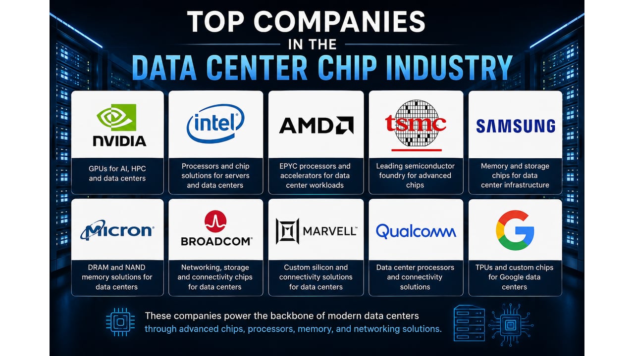
Accelerator density illustrates the industry's technical scale. NVIDIA's current Vera Rubin NVL72 architecture integrates 72 Rubin GPUs and 36 Vera CPUs in a rack-scale system, while AMD's Helios platform also uses 72 GPUs and provides 31 TB of aggregate HBM4 memory. Google's seventh-generation Ironwood TPU architecture scales to 9,216 accelerator chips in a pod. Intel's Xeon 6+ portfolio reaches 288 efficiency cores in a single processor, demonstrating that general-purpose server CPUs are simultaneously moving toward higher consolidation density. Competition therefore extends beyond individual chips into complete rack, memory, interconnect, cooling, compiler, and software ecosystems.
Market Evolution and Growth Drivers
Data-center silicon has evolved from predominantly CPU-centric architectures into heterogeneous computing systems combining CPUs, GPUs, AI accelerators, DPUs, custom ASICs, memory controllers, switches, optical interfaces, and specialized inference processors. U.S. data-center electricity consumption increased from 58 TWh in 2014 to 176 TWh in 2023, reaching 4.4% of national electricity use. That operational shift has increased demand for processors capable of delivering greater compute output within constrained rack power and thermal envelopes. AI has accelerated the change because large models require parallel matrix computation, high-speed memory access, low-latency accelerator communication, and sophisticated distributed-computing software rather than CPU performance alone.
Semiconductor manufacturing technology is another major adoption driver. Intel Xeon 6+ processors introduced Intel 18A into data-center CPUs in 2026, AMD's MI455X accelerator uses advanced 2 nm and 3 nm manufacturing technologies, and Fujitsu has announced a 2 nm process for its MONAKA data-center processor scheduled for 2027. At the system level, high-density liquid cooling is becoming more important because a Xeon 6+ rack configuration can provide 36,864 CPU cores while operating at roughly 100 kW. These developments show why the Top Companies in the Data Center Chip Industry increasingly compete on process nodes, packaging, memory bandwidth, energy efficiency, thermal engineering, and system integration at the same time.
Top 5 Latest Trends in the Data Center Chip Industry
The 5 major current trends influencing data-center silicon development are:
Rack-scale AI accelerator architectures
HBM4, chiplets, and advanced semiconductor integration
Hyperscaler-designed custom AI silicon
High-bandwidth Ethernet and optical interconnects
Heterogeneous CPU and accelerator computing
Trend 1: Rack-Scale AI Accelerator Architectures
Rack-scale computing has become commercially important because modern AI models frequently require dozens of tightly interconnected accelerators to behave as a unified compute domain. NVIDIA's Vera Rubin NVL72 configuration combines 72 GPUs with 36 CPUs and provides 20.7 TB of HBM4 capacity, while its rack architecture delivers 260 TB/s of NVLink 6 switching bandwidth. AMD's Helios design similarly integrates 72 MI455X GPUs, provides 31 TB of aggregate HBM4, and delivers 1.67 PB/s of aggregate memory bandwidth. Instead of optimizing only a single accelerator card, suppliers now engineer processors, switches, memory, power delivery, liquid cooling, firmware, and software as one rack-scale product. This trend is especially relevant to frontier AI training, inference factories, cloud providers, and sovereign AI infrastructure.
Trend 2: HBM4, Chiplets, and Advanced Semiconductor Integration
Memory bandwidth is becoming as important as arithmetic throughput for AI accelerators. NVIDIA's Rubin GPU integrates 336 billion transistors with 288 GB of HBM4 and memory bandwidth reaching 22 TB/s. AMD's MI455X contains 320 billion transistors, 432 GB of HBM4, and 23.3 TB/s of memory bandwidth. Advanced integration is also moving memory functions closer to custom processors: Marvell's 2 nm custom SRAM technology supports configurations reaching 6 gigabits and is designed to reduce total die area by as much as 15% while cutting SRAM standby power by as much as 66%. These specifications explain why chiplets, stacked memory, custom SRAM, advanced packaging, and leading-edge process nodes are central competitive factors among major data center chip manufacturers in 2026.
Trend 3: Hyperscaler-Designed Custom AI Silicon
Large cloud operators are increasingly designing accelerators for their own workloads instead of depending exclusively on merchant GPUs. Google's seventh-generation Ironwood TPU scales to 9,216 liquid-cooled chips per pod, delivering 42.5 exaFLOPS of aggregate compute capability. Each TPU7x chip includes 192 GiB of HBM, 7,380 GB/s of memory bandwidth, and 1,200 GB/s of bidirectional inter-chip bandwidth. Amazon's Trainium3 UltraServer architecture supports as many as 144 Trainium3 chips and provides 20.7 TB of aggregate HBM3e memory. Custom silicon allows hyperscalers to coordinate hardware with compilers, networking, cloud orchestration, and model-serving software, creating a distinct competitive layer within the Top Companies in the Data Center Chip Industry and increasing demand for semiconductor design, packaging, foundry, and IP partners.
Trend 4: High-Bandwidth Ethernet and Optical Interconnects
The performance of an AI cluster increasingly depends on how effectively thousands of accelerators communicate. Broadcom's Tomahawk 6 Ethernet switch entered production-volume shipments in 2026 with 102.4 Tbps of switching capacity, twice the bandwidth of the preceding generation. Its architecture can support scale-up connectivity for 512 XPUs and two-tier scale-out networks containing over 100,000 XPUs using 200 Gbps links. Marvell is simultaneously developing co-packaged-optics technologies intended to extend accelerator connectivity from tens of processors in a rack to hundreds across racks; its silicon-photonics technology has accumulated over 10 billion device-hours of field operation. Networking chips, SerDes, optical DSPs, silicon photonics, and co-packaged optics are therefore moving closer to the center of data-center chip architecture.
Trend 5: Heterogeneous CPU and Accelerator Computing
The AI era has not eliminated server CPUs; it has changed their role. Intel Xeon 6+ processors provide as many as 288 efficiency cores, 12 DDR5 memory channels, and 96 PCIe Gen5 lanes, allowing servers to host dense general-purpose workloads while feeding external accelerators. Arm's Neoverse N3 platform can scale from 8 to 192 cores and delivers a reported 20% performance-per-watt improvement over Neoverse N2, with machine-learning performance approaching 3 times that of the preceding platform in Arm's measurements. IBM's Spyre accelerator complements enterprise CPUs with 32 accelerator cores, 128 GB of LPDDR5 memory, and PCIe Gen5 connectivity. These architectures demonstrate the movement toward workload-specific combinations of CPUs and accelerators rather than a single universal data-center processor.
Top 10 Companies in the Data Center Chip Industry
The following 10 major companies in the Data Center Chip industry are presented based on product capabilities, technical expertise, innovation, deployment scale, geographic presence, and direct relevance to data-center computing. The sequence is not a strict market-share ranking.
1. NVIDIA
Company Overview: NVIDIA was founded in 1993 and operates from its corporate headquarters in Santa Clara, California, United States. Its international footprint includes over 50 offices spanning the Americas, Asia, and Europe. The company's transition from graphics processing to accelerated computing has positioned its GPUs and networking platforms across AI training, AI inference, high-performance computing, and cloud infrastructure.
Headquarters: Santa Clara, California, United States.
Core Data Center Chip Expertise: NVIDIA develops data-center GPUs, CPUs, networking silicon, interconnects, DPUs, switches, and rack-scale AI systems. The Rubin GPU contains 336 billion transistors and delivers HBM4 memory bandwidth reaching 22 TB/s, illustrating the company's focus on highly parallel compute coupled with extremely high memory throughput.
Major Products and Services: The 2026 Vera Rubin platform combines Rubin GPUs, Vera CPUs, NVLink 6, networking, and rack-scale infrastructure. A Rubin NVL72 configuration contains 72 GPUs and 36 CPUs with 20.7 TB of HBM4, making the platform relevant to hyperscale AI factories, cloud services, scientific computing, and large-model inference.
2. AMD
Company Overview: Advanced Micro Devices was founded in 1969 and maintains executive offices in Santa Clara, California. Its global engineering and operational footprint includes major locations in the United States, Canada, Ireland, China, Singapore, and India, supporting CPU, GPU, adaptive-computing, and data-center product development.
Headquarters: Santa Clara, California, United States.
Core Data Center Chip Expertise: AMD combines EPYC server CPUs with Instinct data-center accelerators and rack-scale AI platforms. Its MI455X accelerator uses CDNA 5 architecture, advanced 2 nm and 3 nm manufacturing technologies, 320 billion transistors, and 432 GB of HBM4 memory.
Major Products and Services: AMD's Helios rack-scale system connects 72 MI455X accelerators and supplies 31 TB of HBM4 with aggregate bandwidth of 1.67 PB/s. The architecture extends AMD's competitive position from standalone CPUs and accelerator cards into integrated AI infrastructure for model training and inference.
3. Intel
Company Overview: Intel was founded in 1968 and is headquartered in Santa Clara, California. Its data-center semiconductor activities span processor architecture, silicon manufacturing, packaging, networking, accelerators, and platform development, giving the company direct control over multiple stages of server-chip production.
Headquarters: Santa Clara, California, United States.
Core Data Center Chip Expertise: Intel's Xeon product line remains focused on cloud, enterprise, telecommunications, storage, analytics, and AI-support workloads. Xeon 6+ processors introduced Intel 18A process technology to server CPUs in 2026 and scale to 288 efficiency cores per socket with cache capacity reaching 576 MB.
Major Products and Services: Xeon 6+ supports 12 DDR5 memory channels and 96 PCIe Gen5 lanes, while Intel states that selected configurations can achieve server-consolidation ratios reaching 9:1 in suitable workloads. A liquid-cooled rack can provide 36,864 CPU cores with 384 TB of DDR5 memory, demonstrating Intel's emphasis on density as well as individual processor performance.
4. Broadcom
Company Overview: Broadcom's semiconductor heritage spans over 60 years, while the present corporate organization operates from Palo Alto, California. Its data-center portfolio covers switching silicon, Ethernet PHYs, SerDes, optical connectivity, custom accelerators, storage connectivity, and infrastructure semiconductor technologies.
Headquarters: Palo Alto, California, United States.
Core Data Center Chip Expertise: Broadcom is particularly important in AI-cluster networking and custom silicon. The Tomahawk 6 Ethernet switch provides 102.4 Tbps of switching capacity and supports 100G and 200G PAM4 SerDes, addressing bandwidth requirements created by large GPU and XPU clusters.
Major Products and Services: Production-volume shipments of Tomahawk 6 began in 2026. Its architecture is designed for 512-XPU scale-up domains and two-tier scale-out fabrics containing over 100,000 XPUs, making switching silicon a direct performance component of modern AI data-center architecture rather than a secondary connectivity layer.
5. Marvell Technology
Company Overview: Marvell was founded in 1995 and has developed into a data-infrastructure semiconductor specialist. Its current corporate filing identifies Wilmington, Delaware, as its headquarters, while its Santa Clara operation remains an important U.S. semiconductor engineering location; international operations include sites across Asia, Europe, Israel, and the Americas.
Headquarters: Wilmington, Delaware, United States.
Core Data Center Chip Expertise: Marvell develops custom compute silicon, networking processors, electro-optics, DSPs, storage controllers, interconnect technologies, and semiconductor IP. Its 2 nm custom SRAM platform can integrate as much as 6 gigabits of high-speed embedded memory while reducing total die area by as much as 15%.
Major Products and Services: Marvell's data-center roadmap includes 2 nm custom XPUs, CPUs, switches, co-packaged optics, and silicon-photonics technologies. Its silicon-photonics platform has accumulated over 10 billion device-hours of field operation, supporting the transition toward optical links as electrical connections encounter distance, bandwidth, and power limitations.
6. Arm
Company Overview: Arm originated in 1990 with a team of 12 chip designers and is headquartered in Cambridge, United Kingdom. Unlike companies focused primarily on selling finished processors, Arm licenses processor architectures and computing subsystems used by semiconductor suppliers and cloud infrastructure developers.
Headquarters: Cambridge, United Kingdom.
Core Data Center Chip Expertise: Arm's Neoverse architecture targets cloud, hyperscale, networking, edge infrastructure, and custom data-center processors. Neoverse N3 scales from 8 to 192 cores and provides 2 MB of L2 cache per core, allowing licensees to configure processors for different compute-density requirements.
Major Products and Services: Neoverse N3 delivers a reported 20% improvement in performance per watt compared with N2, while Arm's CSS platforms provide pre-integrated compute subsystems intended to shorten custom-chip development cycles. The Neoverse ecosystem therefore enables hyperscalers and semiconductor companies to create differentiated server CPUs without designing every processor component from the beginning.
7. Google
Company Overview: Google was founded in 1998 and is headquartered in Mountain View, California. Within Alphabet, Google has developed multiple generations of Tensor Processing Units specifically for cloud AI, moving hyperscale infrastructure from exclusive dependence on merchant processors toward internally designed accelerator silicon.
Headquarters: Mountain View, California, United States.
Core Data Center Chip Expertise: Google's seventh-generation Ironwood TPU, identified as TPU7x, incorporates 2 TensorCores and 4 SparseCores per chip. Each device provides 192 GiB of HBM and 7,380 GB/s of memory bandwidth, with high-speed inter-chip connectivity designed for large distributed AI workloads.
Major Products and Services: Ironwood became generally available in 2026 and can scale to 9,216 liquid-cooled chips in a pod, producing 42.5 exaFLOPS of aggregate compute capability. Google deploys the processors through its cloud infrastructure, making software, compiler optimization, networking, storage, and custom silicon components of a single AI-computing environment.
8. IBM
Company Overview: IBM traces its corporate formation to 1911 and adopted the International Business Machines name in 1924. Its headquarters is in Armonk, New York, and its semiconductor-related data-center expertise centers on enterprise processors and accelerators used in IBM Z, LinuxONE, and Power systems.
Headquarters: Armonk, New York, United States.
Core Data Center Chip Expertise: IBM develops processors for transaction processing, enterprise AI, mainframe computing, high-availability infrastructure, and regulated workloads. Its Spyre accelerator contains 32 accelerator cores, uses a 5 nm manufacturing process, and operates within a 75 W PCIe card power envelope.
Major Products and Services: Spyre cards provide 128 GB of LPDDR5 memory and PCIe Gen5 x16 connectivity. IBM supports configurations containing as many as 48 accelerator cards in IBM Z and LinuxONE environments and 16 cards in Power systems, illustrating a specialization strategy centered on integrating AI inference with established enterprise computing platforms.
9. Cerebras Systems
Company Overview: Cerebras Systems was founded in 2015 and is headquartered in Sunnyvale, California. The company's semiconductor strategy differs from conventional reticle-sized GPUs by using wafer-scale processors designed to minimize communication overhead between individual AI compute cores.
Headquarters: Sunnyvale, California, United States.
Core Data Center Chip Expertise: The 2026 WSE-3T wafer-scale processor contains 4 trillion transistors and 900,000 AI cores on a 46,225 mm² silicon device. It integrates 44 GB of on-wafer SRAM and provides memory bandwidth reaching 43.2 PB/s, giving Cerebras a technically distinct position among global Data Center Chip technology providers.
Major Products and Services: WSE-3T powers the CS-4 AI system and provides 250 PFLOPS of wafer-level compute capability. Cerebras announced initial CS-4 shipments for the third quarter of 2026, extending its wafer-scale architecture into a new generation intended for AI inference and large-model workloads.
10. Fujitsu
Company Overview: Fujitsu was established on June 20, 1935 and currently maintains its corporate headquarters at Fujitsu Technology Park in Kawasaki, Kanagawa, Japan. Its processor-development history includes high-performance computing systems and Arm-based server silicon used for technically demanding scientific workloads.
Headquarters: Kawasaki, Kanagawa, Japan.
Core Data Center Chip Expertise: Fujitsu's A64FX processor integrates 48 compute cores plus 4 assistant cores, uses a 7 nm process, incorporates 32 GiB of HBM2, and contains 8.7 billion transistors. Memory bandwidth exceeds 1 TB/s through 4 HBM2 stacks, supporting memory-intensive HPC workloads.
Major Products and Services: Fujitsu is developing the 2 nm MONAKA processor for introduction in 2027. The announced processor is intended for AI, database, and general-purpose data-center workloads and represents Fujitsu's planned extension from HPC-oriented silicon toward broader energy-efficient server computing.
Regional Outlook
North America
North America combines hyperscale chip design, cloud deployment, AI infrastructure, and a renewed semiconductor-manufacturing strategy. U.S. data centers consumed 176 TWh of electricity in 2023, corresponding to 4.4% of national electricity consumption, making processor efficiency and compute density direct infrastructure priorities. The United States hosts the headquarters of NVIDIA, AMD, Intel, Google, IBM, Broadcom, and Cerebras among the 10 companies profiled here, giving the region extensive expertise in GPUs, CPUs, TPUs, Ethernet switching, wafer-scale processors, and enterprise accelerators. Federal semiconductor policy also targets at least 2 new large-scale leading-edge logic manufacturing clusters by the end of the decade, alongside additional advanced-packaging capacity.
Canada's opportunity is tied increasingly to sovereign AI compute and electricity availability. Federal planning estimates that Canadian commercial participants could require 5.5 GW of AI-compute infrastructure by 2030, while individual AI data centers are increasingly being planned at scales of at least 100 MW. Canada's semiconductor ecosystem also includes advanced-packaging activities, including the Bromont cluster, but the country still depends heavily on global manufacturing capacity for leading AI processors. These conditions create opportunities in accelerator deployment, packaging, cooling, electrical infrastructure, and domestic AI-compute services rather than only leading-edge wafer fabrication.
Mexico is developing an earlier-stage semiconductor design and supply-chain position. The Kutsari initiative launched in 2025 with design-center activity in Puebla, Jalisco, and Sonora and a stated objective of consolidating chip-design capabilities by 2027. Plans have also outlined development of a domestic manufacturing model during 2026 and longer-term fabrication capability toward 2029. Mexico's education system has 184,000 students in technical programs linked to semiconductor-relevant disciplines, providing a workforce foundation that could support design, validation, assembly, testing, and electronics manufacturing as North American supply chains become more localized.
Europe
Europe's data-center chip position combines processor intellectual property, semiconductor equipment, research institutions, advanced manufacturing programs, cloud expansion, and strict energy-efficiency regulation. The European Union accounted for 9% of the global semiconductor market in 2026 data cited by the European Commission, compared with its policy ambition of reaching 20% by 2030. The European Chips Act supports expansion across the 27 EU member states, while the United Kingdom contributes globally important processor architecture through Arm in Cambridge. Arm's Neoverse N3 can scale to 192 cores, illustrating Europe's continuing role in the processor IP that underpins cloud and custom data-center CPUs even when physical wafer production occurs in another region.
Energy regulation is becoming a distinctive European competitive factor. Under the recast Energy Efficiency Directive adopted in 2023, data centers with installed information-technology power demand above 500 kW fall within mandatory reporting requirements established through the EU framework. Regulatory categories extend from facilities in the 100–500 kW band to installations above 10 MW, creating standardized visibility into energy and sustainability performance. Germany, France, Italy, Spain, the Netherlands, and Nordic EU markets operate within this regulatory framework, while the United Kingdom follows its own post-EU policy environment. For chip suppliers, European customer demand therefore increasingly connects compute performance with power management, server utilization, cooling efficiency, environmental reporting, and infrastructure transparency.
Europe also contains important design and research specialization even though its leading-edge manufacturing share remains below the 2030 policy objective. Arm was founded by 12 designers in 1990 in the United Kingdom, and its current data-center architectures provide semiconductor companies with configurable CPU intellectual property. At the same time, the European semiconductor-policy agenda is designed to strengthen manufacturing, packaging, design, and research resilience rather than concentrate on a single stage of the supply chain. This structure creates opportunities for data-center chip companies that can connect processor design with advanced packaging, energy-efficient systems, optical networking, and regional manufacturing partnerships.
Asia-Pacific
Asia-Pacific has the deepest manufacturing concentration in the data-center chip supply chain and combines foundry capacity, memory production, advanced packaging, processor design, and rapidly expanding AI infrastructure. China represented 25% of worldwide data-center electricity consumption in 2024, illustrating the operating scale of its cloud and digital infrastructure. Taiwan remains central to advanced semiconductor manufacturing, with 2 nm production expansion progressing in its science-park ecosystem, while South Korea's memory manufacturers are advancing HBM4 and DDR5 technologies required by next-generation accelerators. Japan contributes processor design through Fujitsu, whose planned MONAKA data-center CPU is being developed using a 2 nm manufacturing process for introduction in 2027.
India is moving simultaneously into semiconductor manufacturing and shared AI-compute infrastructure. By February 2026, the country had approved 10 semiconductor manufacturing projects comprising 2 fabrication facilities and 8 packaging-related units, with pilot production underway at 4 units. India's shared AI-compute infrastructure had also expanded beyond 45,000 GPUs by June 2026, while 237 projects had accessed the national compute platform. These developments create demand not only for imported accelerators but also for packaging, validation, server integration, thermal management, networking, software optimization, and eventually greater domestic semiconductor design activity.
Singapore demonstrates how smaller Asia-Pacific economies can compete through concentrated data-center infrastructure rather than wafer fabrication. Its data-center estate contains over 70 facilities with an existing capacity base of 1.4 GW, while the national roadmap provides for at least 300 MW of additional capacity and potentially another 200 MW supported by green-energy arrangements. Singapore has also deployed the ASPIRE 2A and 2A+ research-computing environment with 30 PFLOPS of combined capability. This creates a regional testing and deployment market for accelerators, CPUs, switching chips, optical components, liquid-cooling technologies, and energy-efficient data-center systems serving Southeast Asian customers.
Middle East & Africa
Middle East data-center chip demand is being driven primarily by sovereign AI programs, digital-government infrastructure, cloud localization, and large-scale computing projects. Saudi Arabia had over 60 operational data centers supplied by over 20 companies in 2025, with total operational capacity exceeding 440 MW compared with 68 MW in 2021. National planning targets data-center capacity of 1,300 MW by 2030, while separate AI-compute programs have outlined 1.9 GW of capacity by 2030 and 6 GW by 2034. These targets create direct requirements for GPUs, CPUs, switches, optical interconnects, HBM-intensive accelerators, liquid cooling, and high-density power systems.
Saudi infrastructure is also moving toward individual campuses measured in hundreds of megawatts. Construction activity announced in 2026 for the Hexagon government data-center project covers a planned 480 MW Tier IV facility, illustrating the scale at which regional customers are beginning to specify computing infrastructure. The United Arab Emirates provides another demand center: its national AI strategy dates to 2017 and establishes 2031 as a central government transformation milestone. As Gulf governments integrate AI into public services, energy, transport, healthcare, and national digital platforms, demand shifts from conventional hosting servers toward accelerator-rich systems capable of training and serving AI models locally.
African markets remain less uniform but are developing national AI-policy and infrastructure frameworks. Kenya's national AI strategy covers the 2025–2030 period and explicitly connects AI development with digital infrastructure, data, research, innovation, and skills. South Africa's 2026 draft national AI policy is organized around 6 strategic pillars, demonstrating a parallel effort to formalize national AI capabilities. Import dependence for advanced processors, limited hyperscale availability in some markets, grid constraints, skills shortages, and cooling requirements remain barriers, yet the 2030 policy horizon is creating opportunities for cloud-region expansion, smaller sovereign-compute platforms, accelerator hosting, technical training, and energy-efficient server deployments.
Future Opportunities in the Data Center Chip Industry
Future opportunities for the Top Companies in the Data Center Chip Industry are strongly connected to the widening gap between AI-compute demand and available power, memory bandwidth, networking capacity, and semiconductor manufacturing resources. The International Energy Agency projects global data-center electricity consumption to rise from 485 TWh in 2025 to 950 TWh in 2030, while electricity demand associated specifically with AI-focused data centers is projected to triple during the same period. These are projections rather than present operating figures, but they demonstrate why future chip development will place greater emphasis on performance per watt, lower-precision arithmetic, memory efficiency, power management, liquid cooling, and workload-specific acceleration.
Verified technology roadmaps show where semiconductor innovation is heading. Fujitsu plans to introduce its 2 nm MONAKA processor in 2027, while NVIDIA's Rubin generation already moves accelerator memory to HBM4 with 22 TB/s bandwidth and AMD's MI455X reaches 23.3 TB/s. Broadcom's 102.4 Tbps Tomahawk 6 and Marvell's co-packaged-optics work demonstrate that networking is developing alongside compute because scaling thousands of accelerators requires corresponding increases in fabric bandwidth. Commercial opportunity therefore extends beyond GPUs into HBM, custom SRAM, chiplets, advanced substrates, silicon photonics, SerDes, Ethernet switches, optical DSPs, packaging, and thermal-management technology.
Geographic targets provide additional measurable opportunities. The European Union retains a 20% semiconductor-share objective for 2030; Canada estimates commercial AI-compute requirements of 5.5 GW by 2030; Saudi Arabia targets 1,300 MW of data-center capacity by 2030; and Singapore's roadmap provides for at least 300 MW of additional data-center capacity. These verified targets do not guarantee equivalent chip shipments, but analytically they indicate where demand for accelerator servers, custom silicon, networking processors, memory, advanced cooling, and local technical support can expand. Suppliers capable of aligning silicon roadmaps with regional power constraints and data-sovereignty requirements should have a wider set of deployment pathways than vendors competing primarily on peak computational throughput.
A further opportunity lies in design diversification. Google's Ironwood can scale to 9,216 custom TPU chips, Arm Neoverse N3 supports configurations reaching 192 cores, IBM Spyre systems can combine as many as 48 accelerator cards, and Cerebras uses 900,000 AI cores on a single wafer-scale processor. These architectures demonstrate that future data centers are unlikely to converge on 1 universal chip design. Instead, cloud training, enterprise inference, databases, scientific computing, networking, storage, telecommunications, and sovereign AI can support different processor combinations. Custom ASIC design, reusable processor IP, domain-specific accelerators, integrated software stacks, and chip-to-cloud optimization consequently represent realistic opportunities for established suppliers and specialized semiconductor companies.
Conclusion
The Top Companies in the Data Center Chip Industry operate within an increasingly heterogeneous computing environment shaped by 5 major technical trends: rack-scale accelerators, HBM4 and advanced integration, hyperscaler custom silicon, high-bandwidth networking, and mixed CPU-accelerator architectures. NVIDIA and AMD are advancing 72-GPU rack systems; Google scales Ironwood to 9,216 custom accelerators per pod; Intel provides server processors with as many as 288 efficiency cores; Broadcom supplies 102.4 Tbps switching silicon; and Cerebras integrates 4 trillion transistors into its wafer-scale processor. Arm, Marvell, IBM, and Fujitsu add processor IP, custom silicon, optical connectivity, enterprise acceleration, and energy-efficient CPU architectures to an industry that now competes at the full-system level.
Regional conditions remain equally important. The United States recorded data-center electricity demand equal to 4.4% of national consumption in 2023, the European Union is working toward a 20% semiconductor-share objective for 2030, India had approved 10 semiconductor manufacturing projects by early 2026, Singapore operates over 70 data centers, and Saudi Arabia recorded operational data-center capacity above 440 MW in 2025. These differences mean future competition will depend not only on transistor density or peak AI performance but also on semiconductor supply resilience, power efficiency, packaging, memory availability, optical networking, liquid cooling, software ecosystems, regional regulation, and the capacity to deploy silicon reliably across different infrastructure environments.