


Top Companies in the AI Accelerator Chip Industry and Their Key Capabilities
The top companies in the AI accelerator chip industry are examined by products, technical strengths, regional reach, current trends, and future opportunities.
Introduction
Overview of the Global AI Accelerator Chip Industry
The global AI accelerator chip industry in 2026 includes graphics processing units, tensor processing units, neural processing units, inference ASICs, wafer-scale processors, and purpose-built cloud accelerators. Hardware configurations now range from 75-watt and 150-watt PCIe cards to liquid-cooled systems containing 72 interconnected accelerators. Google’s seventh-generation Ironwood architecture scales to 9,216 chips in 1 pod, Amazon Trainium3 UltraServers integrate as many as 144 chips, and NVIDIA’s Vera Rubin NVL72 combines 72 Rubin GPUs with 36 Vera CPUs. These configurations illustrate how the industry has progressed from individual processors to complete computing systems optimized for training, fine-tuning, reasoning, and real-time inference.
Demand for AI accelerators is concentrated in cloud computing, generative AI, recommendation systems, autonomous machines, industrial inspection, telecommunications, healthcare, financial services, scientific research, and government infrastructure. Meta reported in March 2026 that hundreds of thousands of its custom MTIA chips were already supporting inference workloads, while India had onboarded more than 38,000 GPUs through 14 service providers for shared national compute. NVIDIA’s Rubin supply chain spans more than 350 factory sites in 30 countries, demonstrating that AI accelerator production depends on an international network of foundries, memory suppliers, packaging specialists, networking vendors, system integrators, and data-center operators.
The competitive structure of the industry includes merchant semiconductor companies, hyperscale cloud providers, telecommunications-chip specialists, vertically integrated technology groups, and wafer-scale computing developers. Accelerator specifications in 2026 extend from Qualcomm’s 150-watt Cloud AI 100 Ultra card to AMD’s 432 GB HBM4 MI455X and Cerebras’ 4-trillion-transistor Wafer-Scale Engine 3. This diversity allows customers to select hardware according to model size, numerical precision, latency, power availability, software compatibility, deployment location, and scale-out requirements rather than relying on 1 processor architecture for every workload.
Market Evolution and Growth Drivers
The AI accelerator chip industry has evolved through multiple overlapping product generations. Huawei introduced the Ascend 310 in 2018 and Ascend 910 in 2019, Meta developed its first MTIA family in 2023, Cerebras introduced its 5-nanometer WSE-3 in 2024, and Amazon made its first 3-nanometer Trainium3 chip generally available in December 2025. The 2026 product cycle added Microsoft Maia 200, NVIDIA Rubin, AMD MI455X, and expanded MTIA deployments. These launches show that commercial significance has shifted from general-purpose parallel processing toward workload-specific silicon, lower-precision computation, integrated networking, larger memory systems, and complete rack-level architectures.
Model complexity and memory movement are primary technical drivers. One Rubin GPU provides 288 GB of HBM4 with 22 TB/s of bandwidth, while the MI455X provides 432 GB with 23.3 TB/s. Google’s Ironwood offers 192 GiB per chip and 7,380 GB/s, compared with 32 GiB and 1,638 GB/s for the previous Trillium generation. These increases allow more model weights, key-value caches, activations, and expert layers to remain close to the compute engines. Lower-precision formats such as FP8, FP6, FP4, MXFP8, and MXFP4 are also increasing throughput while reducing memory and energy requirements for training and inference.
Government compute programs and semiconductor policies are accelerating adoption beyond large technology companies. The European Union is developing 19 AI Factories across 16 member states, the United Kingdom intends to expand public AI compute capacity by at least 20 times by 2030, and India has moved from an initial target of 10,000 GPUs to more than 38,000 onboarded units. These programs are expanding accelerator access for universities, public agencies, start-ups, and small enterprises that cannot independently operate hyperscale clusters.
Top 5 Latest Trends in the AI Accelerator Chip Industry
Rack-scale AI systems and co-designed computing infrastructure
HBM4 adoption, chiplets, and advanced packaging
Low-precision acceleration for high-volume inference
Hyperscaler-designed custom AI silicon
Energy-efficient edge and sovereign AI deployment
Trend 1: Rack-Scale AI Systems and Co-Designed Computing Infrastructure
Rack-scale architecture has become commercially important because frontier models require hundreds or thousands of accelerators to behave as a single coordinated machine. NVIDIA’s Vera Rubin NVL72 combines 72 GPUs, 36 CPUs, NVLink 6 switching, liquid cooling, and 260 TB/s of rack-level NVLink bandwidth. AMD Helios similarly integrates 72 MI455X GPUs and provides up to 31 TB of HBM4 with 1.67 PB/s of aggregate memory bandwidth. Amazon’s Trainium3 UltraServer scales to 144 chips, while Google Ironwood supports a 3-dimensional torus topology containing as many as 9,216 chips. Top Companies in the AI Accelerator Chip Industry are therefore competing through processors, networking, cooling, software, power management, serviceability, and complete system blueprints rather than isolated benchmark results.
Trend 2: HBM4 Adoption, Chiplets, and Advanced Packaging
Memory bandwidth has become a central accelerator-design constraint because processing units can remain underutilized when model parameters and activations cannot be delivered quickly enough. The 2026 Rubin GPU contains 288 GB of HBM4 delivering 22 TB/s, while AMD’s MI455X integrates 12 HBM4 stacks providing 432 GB and 23.3 TB/s. Samsung’s HBM4 uses a 4-nanometer logic base die and supports speeds of up to 13 Gbps with maximum bandwidth of 3.3 TB/s per stack. Chiplets and 3-dimensional hybrid bonding allow compute, cache, memory, and input/output functions to use different manufacturing processes. These techniques improve design flexibility but increase dependence on advanced substrates, bonding, thermal interfaces, interposers, testing systems, and high-yield packaging capacity.
Trend 3: Low-Precision Acceleration for High-Volume Inference
Inference-specialized computing is expanding as AI applications move from model development to billions or trillions of production requests. Microsoft Maia 200 supports native FP8 and FP4 formats, provides more than 10 PFLOPS at FP4 precision, and connects clusters containing as many as 6,144 accelerators. NVIDIA Rubin reaches 50 PFLOPS of NVFP4 inference per GPU, while AMD MI455X reaches 40.3 PFLOPS of MXFP4 performance. Qualcomm approaches inference through a 150-watt PCIe card that supplies up to 870 TOPS of INT8 processing and can accommodate a 100-billion-parameter model on 1 card. These designs reduce unnecessary numerical precision while retaining suitable model accuracy through quantization, sparsity, calibration, and precision-aware software tools.
Trend 4: Hyperscaler-Designed Custom AI Silicon
Cloud and platform companies are designing accelerators around their own workloads, software stacks, networking systems, and data-center operating models. Google’s TPU7x Ironwood provides 4,614 TFLOPS of FP8 compute per chip and scales to 9,216 chips. Amazon Trainium3 provides 2.52 PFLOPS of FP8 compute with 144 GB of HBM3e, while Microsoft Maia 200 combines 216 GB of HBM3e, 272 MB of on-chip SRAM, and clusters of up to 6,144 accelerators. Meta is developing MTIA 300, 400, 450, and 500 within a 2-year roadmap and has shortened its design cadence to approximately 6 months or less. Custom silicon gives hyperscalers tighter control over workload optimization, software integration, capacity planning, supply diversification, and energy efficiency.
Trend 5: Energy-Efficient Edge and Sovereign AI Deployment
AI acceleration is spreading beyond centralized hyperscale facilities into factories, telecommunications networks, government systems, vehicles, hospitals, and private enterprise infrastructure. Qualcomm’s Cloud AI 100 Ultra delivers up to 870 TOPS at 150 watts, while its industrial IQ-9075 platform supports up to 100 dense TOPS, as many as 16 camera inputs, and operating temperatures from minus 40°C to 115°C. Sovereign deployments are expanding simultaneously: India is adding 20,000 GPUs beyond its existing 38,000-unit shared-compute pool, Europe is establishing 19 AI Factories, and Canada estimates that commercial users could require 5.5 GW of AI compute by 2030. These developments create demand for accelerators that support data residency, predictable power use, secure offline operation, open software, and localized technical support.
Top 10 Companies in the AI Accelerator Chip Industry
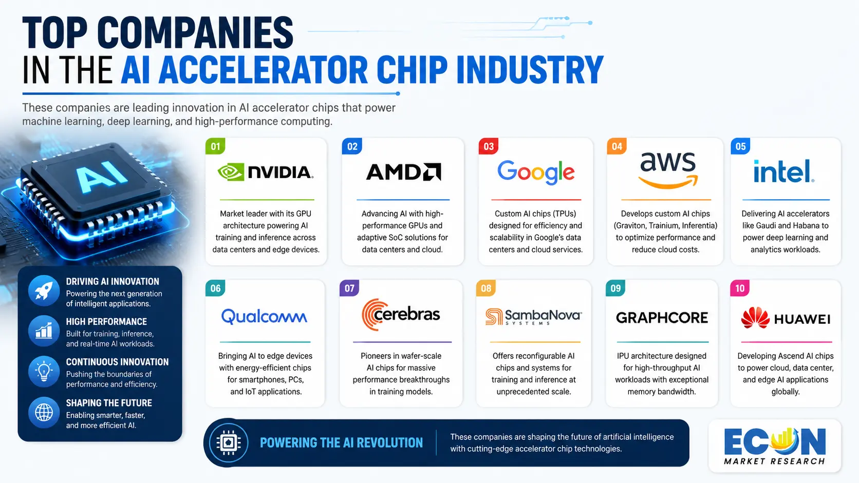
The following 10 companies are not presented as a strict ranking. They were selected according to active accelerator products, technical capabilities, deployment scale, software ecosystems, geographic relevance, manufacturing partnerships, and contribution to AI computing infrastructure.
1. NVIDIA Corporation
Company Overview: NVIDIA was founded on April 5, 1993, by Jensen Huang, Chris Malachowsky, and Curtis Priem. Its activities have expanded from 3-dimensional graphics into data-center accelerators, networking, CPUs, automotive computing, robotics, digital twins, and AI software. Headquarters: The company is headquartered in Santa Clara, California, United States, and its 2026 Rubin supply network involves more than 350 factory sites across 30 countries.
Core AI Accelerator Chip Expertise: NVIDIA combines GPU architecture, Tensor Cores, high-speed interconnects, networking, CUDA software, compilers, optimized libraries, and rack-level engineering. Major Products and Services: The Vera Rubin NVL72 integrates 72 Rubin GPUs and 36 Vera CPUs, providing up to 3,600 PFLOPS of NVFP4 inference, 20.7 TB of HBM4, and 260 TB/s of NVLink 6 switch bandwidth. Each Rubin GPU contains 336 billion transistors, 896 Tensor Cores, 288 GB of HBM4, and up to 22 TB/s of memory bandwidth.
2. Advanced Micro Devices, Inc.
Company Overview: AMD was founded in 1969 as a Silicon Valley semiconductor start-up. Its accelerator activities are supported by operations in locations including Santa Clara, Austin, San Jose, Shanghai, Markham, Dublin, Singapore, Bengaluru, and Hyderabad. Headquarters: AMD’s corporate headquarters is in Santa Clara, California, United States.
Core AI Accelerator Chip Expertise: AMD develops chiplet-based data-center GPUs, high-performance CPUs, adaptive computing products, networking technologies, and the ROCm software ecosystem. Major Products and Services: Launched on July 23, 2026, the MI455X uses 2-nanometer and 3-nanometer manufacturing technologies, contains 320 billion transistors, and supplies 40.3 PFLOPS of MXFP4 performance. Its 432 GB of HBM4 delivers 23.3 TB/s, while 72 MI455X accelerators form an AMD Helios rack with as much as 2.9 exaFLOPS of MXFP4 compute.
3. Intel Corporation
Company Overview: Intel was founded in 1968 and has contributed to semiconductor manufacturing, CPUs, memory, networking, programmable devices, and computing standards for more than 55 years. Headquarters: The company’s global headquarters is in Santa Clara, California, United States. Its AI accelerator portfolio is designed to support enterprise, cloud, scientific, and on-premises deployments.
Core AI Accelerator Chip Expertise: Intel focuses on programmable tensor processors, Ethernet-based scaling, open software, PyTorch integration, and enterprise system compatibility. Major Products and Services: Gaudi 3 contains 64 programmable tensor processor cores, 8 matrix multiplication engines, 128 GB of HBM2e, 3.7 TB/s of memory bandwidth, and 24 integrated 200 Gb Ethernet ports. Its configurations range from 1 node with 8 accelerators to clusters containing thousands of units, allowing customers to scale without relying on a proprietary networking fabric.
4. Google
Company Overview: Google was incorporated in 1998 after beginning as a university research project, and its infrastructure activities now include search, cloud computing, machine learning, mobile platforms, and data-center engineering. The company maintains offices in more than 60 countries and operates more than 180 internet domains. Headquarters: Google’s main headquarters, the Googleplex, is in Mountain View, California, United States.
Core AI Accelerator Chip Expertise: Google develops custom Tensor Processing Units, inter-chip networking, compiler technologies, JAX support, Kubernetes integration, and AI-optimized cloud infrastructure. Major Products and Services: TPU7x Ironwood is Google’s seventh TPU generation and supports 9,216 chips per pod. Each chip provides 4,614 TFLOPS of FP8 compute, 192 GiB of HBM, 7,380 GB/s of memory bandwidth, 2 TensorCores, 4 SparseCores, and 1,200 GB/s of bidirectional inter-chip bandwidth.
5. Amazon Web Services
Company Overview: Amazon Web Services began its modern cloud infrastructure operations with the launch of Amazon S3 in 2006. It now operates cloud offices and infrastructure locations across North America, Latin America, Europe, the Middle East, Africa, and Asia-Pacific. Headquarters: AWS is part of Amazon and maintains its principal corporate presence in Seattle, Washington, United States.
Core AI Accelerator Chip Expertise: AWS designs custom training and inference silicon, server systems, scale-out networking, compilers, and cloud services integrated with its EC2 platform. Major Products and Services: Trainium3 became generally available on December 2, 2025, as the first 3-nanometer AWS AI chip. Each chip offers 2.52 PFLOPS of FP8 compute, 144 GB of HBM3e, and 4.9 TB/s of memory bandwidth. A 144-chip Trn3 UltraServer provides 362 FP8 PFLOPS, 20.7 TB of memory, and 706 TB/s of aggregate memory bandwidth.
6. Microsoft Corporation
Company Overview: Microsoft was founded in 1975 and moved to its Redmond corporate campus in 1986. Its technology operations now cover cloud services, enterprise software, developer tools, operating systems, gaming, security, and artificial intelligence. Headquarters: Microsoft is headquartered in Redmond, Washington, United States, where its original headquarters campus opened with 6 buildings on approximately 30 acres.
Core AI Accelerator Chip Expertise: Microsoft develops Azure-specific accelerators, networking systems, firmware, compiler tools, and heterogeneous infrastructure combining internal silicon with third-party hardware. Major Products and Services: Maia 200, introduced on January 26, 2026, uses TSMC’s 3-nanometer process and contains more than 100 billion transistors. It provides more than 10 PFLOPS at FP4, over 5 PFLOPS at FP8, 216 GB of HBM3e operating at 7 TB/s, and 272 MB of on-chip SRAM. Standard Ethernet-based clusters can scale to 6,144 Maia 200 accelerators.
7. Qualcomm Incorporated
Company Overview: Qualcomm was established in 1985 by 7 former Linkabit colleagues and has developed semiconductor, wireless, connectivity, automotive, edge-computing, and AI technologies for approximately 40 years. The company reports 170 offices across more than 30 countries. Headquarters: Qualcomm is headquartered in San Diego, California, United States.
Core AI Accelerator Chip Expertise: Qualcomm specializes in power-efficient inference, on-device AI, industrial edge computing, computer vision, natural-language processing, and private on-premises deployment. Major Products and Services: The Cloud AI 100 Ultra integrates 64 AI cores, 576 MB of SRAM, 128 GB of LPDDR4x memory, and 548 GB/s of memory bandwidth. It supplies up to 870 TOPS of INT8 or 288 TFLOPS of FP16 performance at 150 watts and can support a 100-billion-parameter model on 1 card or a 175-billion-parameter model on 2 cards.
8. Huawei Technologies Co., Ltd.
Company Overview: Huawei was founded in Shenzhen in 1987 and had approximately 213,000 employees at the end of 2025, including 114,000 personnel working in research and development. The company operates in more than 170 countries and regions and serves over 3 billion people through its broader ICT portfolio. Headquarters: Huawei is headquartered in Shenzhen, China.
Core AI Accelerator Chip Expertise: Huawei develops Ascend processors, AI servers, SuperPoD systems, cloud instances, networking, compilers, and the CANN software platform. Major Products and Services: The Atlas 900 A3 SuperPoD, launched in March 2025, integrates up to 384 Ascend 910C chips and delivers as much as 300 PFLOPS. Huawei reported deploying more than 300 systems for over 20 customers. Its roadmap includes Ascend 950, 960, and 970 products, with planned FP4 performance ranging from 2 PFLOPS to 8 PFLOPS per chip.
9. Cerebras Systems, Inc.
Company Overview: Cerebras was incorporated in April 2016 as a developer of AI computing systems and wafer-scale processors. Its systems have been selected by corporations, research institutes, and government organizations on 4 continents for cloud and on-premises deployments. Headquarters: Cerebras is headquartered in Sunnyvale, California, United States.
Core AI Accelerator Chip Expertise: Cerebras designs processors using an entire silicon wafer, eliminating many communication boundaries created by conventional packaged chips. Major Products and Services: The 5-nanometer WSE-3 contains 4 trillion transistors, 900,000 AI-optimized cores, 44 GB of on-chip SRAM, and 125 PFLOPS of peak AI performance. A CS-3 system uses 1 WSE-3, while configurations can scale to 2,048 CS-3 nodes and 256 exaFLOPS. Cerebras and G42 have also used CS-3 systems in the 8-exaFLOPS Condor Galaxy 3 supercomputer.
10. Meta Platforms, Inc.
Company Overview: Meta was established as Facebook in February 2004 and now operates social, messaging, virtual-reality, recommendation, advertising, and generative-AI platforms. Its internal workloads include billions of daily user interactions and trillions of inference requests. Headquarters: Meta is headquartered in Menlo Park, California, United States, where it has maintained its principal corporate campus since 2011.
Core AI Accelerator Chip Expertise: Meta develops workload-specific accelerators for ranking, recommendation, advertising, training, and generative inference. Major Products and Services: The first MTIA family appeared in 2023, and hundreds of thousands of MTIA chips were deployed by March 2026. MTIA 300 entered production for training, while MTIA 400, 450, and 500 are intended to support broader workloads through 2027. Meta’s next-generation custom-silicon program includes an initial deployment commitment exceeding 1 GW and uses software standards such as PyTorch, Triton, vLLM, and Open Compute Project specifications.
Regional Outlook
North America
North America combines accelerator design companies, cloud platforms, AI research organizations, system integrators, and an expanding semiconductor research infrastructure. In the United States, the National Semiconductor Technology Center is establishing 3 flagship facilities: an administrative and design facility, an extreme-ultraviolet research center, and an advanced-packaging prototyping facility. The planned operating milestones were 2025 for the design facility, 2026 for the EUV center, and 2028 for the packaging facility. The NSTC passed 100 members in February 2025, bringing together semiconductor manufacturers, equipment companies, universities, start-ups, and government laboratories.
The United States also contains the headquarters of all 7 American companies profiled in this article, giving the region substantial capabilities in GPU design, cloud ASICs, wafer-scale computing, networking, system software, and inference acceleration. However, production remains globally interdependent because leading accelerators require Asian foundries, HBM suppliers, substrates, optical components, and advanced packaging. The planned Tempe, Arizona, prototyping center is intended to connect 300-millimeter front-end semiconductor processes with advanced packaging research, addressing a gap between laboratory designs and volume manufacturing.
Canada’s sovereign-compute strategy is organized around 3 elements: commercial AI data centers, public supercomputing infrastructure, and a compute-access program. More than 1,000 stakeholders participated in the strategy consultation, and Canada estimates that commercial AI users could require 5.5 GW of compute by 2030. Mexico is strengthening the design side of the supply chain through the Kutsari National Semiconductor Design Center, with initial centers planned in Puebla, Jalisco, and Sonora and consolidation targeted for 2027. Canada’s clean-power availability and Mexico’s automotive and electronics base create opportunities, although both markets remain dependent on imported advanced accelerators.
Europe
Europe’s accelerator strategy combines semiconductor sovereignty, public supercomputing, AI regulation, energy policy, and research access. The European Chips Act entered into force on September 21, 2023, with a policy objective of increasing Europe’s share of global semiconductor production to 20% by 2030. Separately, work has begun on 19 AI Factories across 16 European Union member states, supported by 13 AI Factory Antennas. Most factories are expected to become operational by the end of 2026, connecting supercomputers with universities, start-ups, datasets, training programs, and industrial users.
Germany has more than 2,000 operating data centers with approximately 3 GW of connected capacity and annual electricity consumption of about 20 TWh. A national strategy approved in March 2026 calls for overall data-center capacity to double by 2030 compared with 2025 and for high-performance-computing and AI capacity to increase at least 4 times. Germany also hosts JUPITER, Europe’s first exascale supercomputer, capable of more than 1 quintillion operations per second. These resources support accelerator demand in automotive engineering, industrial automation, pharmaceuticals, climate modeling, and scientific simulation.
The United Kingdom’s AI Research Resource includes Isambard-AI with 5,448 NVIDIA GH200 superchips and Dawn with 1,024 Intel Data Center GPU Max 1550 accelerators. Public AI compute capacity is planned to expand by at least 20 times by 2030, while individual 2026 research projects could request between 50,000 and 1.4 million GPU hours. France, Italy, Spain, the Netherlands, and Nordic countries participate in European supercomputing, AI Factory, semiconductor-research, and energy-efficient data-center initiatives. The regional challenge is balancing accelerator availability with AI Act compliance, electricity constraints, data sovereignty, export controls, and sustainable cooling requirements.
Asia-Pacific
Asia-Pacific is central to AI accelerator manufacturing because Taiwan, South Korea, Japan, China, and Singapore provide advanced foundry capacity, HBM production, packaging, materials, equipment, electronics assembly, and cloud infrastructure. Taiwan began volume production of 2-nanometer technology in the fourth quarter of 2025, with the process designed to provide up to 15% more speed at equal power or 25% to 30% lower power at equal speed than the preceding N3E technology. Japan’s Rapidus program targets advanced logic mass production during fiscal 2027, adding a potential alternative source of leading-edge capacity.
South Korea is combining accelerator procurement with domestic AI-semiconductor development. Its National AI Computing Center planned to secure 10,000 advanced GPUs, while a sixth national supercomputer containing 8,000 GPUs was scheduled for the first half of 2026. The K-Cloud project selected 17 consortia involving 59 institutions, including 37 companies, 15 universities, 3 research institutes, and 4 public or industry organizations. South Korea’s established HBM ecosystem is strategically important because current processors can require 8 to 12 memory stacks per accelerator and several terabytes per second of bandwidth.
India had onboarded more than 38,000 GPUs through 14 service providers by early 2026 and announced the addition of 20,000 more units. Compute facilities operate in cities including Mumbai, Navi Mumbai, Hyderabad, Bengaluru, Noida, and Jamnagar. Singapore reported that SME AI adoption increased from 4.2% in 2023 to 14.5% in 2024, while adoption among larger organizations reached 62.5%. China has developed a vertically integrated accelerator ecosystem led by domestic cloud operators and semiconductor companies; Huawei alone reported more than 300 Atlas 900 A3 deployments for over 20 customers. Regional advantages include manufacturing depth and engineering talent, while risks include export restrictions, geographic concentration, water use, and energy availability.
Middle East & Africa
The Middle East is becoming an important destination for sovereign AI systems because governments are combining digital-transformation programs with new data centers and national-language models. The UAE launched its national AI strategy in 2017 and targets 100% reliance on AI for government services and data analysis by 2031. Its strategy covers 5 implementation themes and sectors including transport, healthcare, energy, water, education, space, and public services. Abu Dhabi-based G42 has partnered with Cerebras on Condor Galaxy systems, including the 8-exaFLOPS CG-3 supercomputer powered by WSE-3 technology.
Saudi Arabia’s data and AI programs are aligned with Vision 2030 and emphasize national capability, research, digital government, responsible data use, and workforce development. The region’s demand is also supported by telecommunications, oil and gas, healthcare, logistics, smart-city, and Arabic-language AI applications. However, accelerator deployments must account for cooling requirements in climates where summer temperatures can exceed 45°C, along with water availability, imported hardware, long component lead times, and a limited pool of engineers experienced in clusters containing thousands of processors.
Africa’s accelerator market remains smaller but is gaining policy and infrastructure foundations. South Africa approved publication of a draft national AI policy in 2026 structured around 6 pillars, including talent, governance, inclusion, and responsible deployment. Kenya’s AI Strategy 2025–2030 contains 3 pillars covering digital infrastructure, data governance, and research commercialization. Nigeria describes its national approach through 5 principles: responsibility, ethics, inclusion, sustainability, and collaboration. These programs can expand demand in agriculture, public health, financial services, education, and government, but limited electricity reliability, cloud concentration, accelerator import dependence, and skills shortages remain material barriers.
Future Opportunities in the AI Accelerator Chip Industry
Future product opportunities will center on memory capacity, low-precision computation, optical and electrical interconnects, advanced packaging, modular chiplets, and energy-aware scheduling. Verified roadmaps already point toward larger systems: Huawei plans Ascend products supporting up to 8 PFLOPS of FP4 performance per chip, Meta intends to introduce 4 MTIA generations within 2 years, and Google Ironwood can scale to 9,216-chip pods. Analytical expectations should remain separate from those verified targets, but these roadmaps indicate that accelerator competition through 2027 will increasingly depend on system-level efficiency, model-specific optimization, software portability, and the ability to operate within fixed power envelopes.
Supply-chain localization offers another opportunity. New facilities for EUV research, 300-millimeter prototyping, HBM4, hybrid bonding, substrates, liquid cooling, and photonic connectivity could reduce geographic concentration across the next 3 to 5 years. Small and medium-sized enterprises will benefit from public compute programs rather than direct ownership of thousands of accelerators; India’s planned pool of more than 58,000 GPUs and Europe’s network of 19 AI Factories demonstrate this access model. Managed inference, reserved accelerator capacity, on-premises appliances, and sovereign-cloud services can also expand adoption among regulated industries requiring local data control.
Energy efficiency will influence both product qualification and customer purchasing. Rubin is designed to deliver up to 10 times the agentic throughput per unit of energy compared with Blackwell, while Qualcomm can execute models containing up to 120 billion parameters on a single 150-watt card. Opportunities therefore exist in lower-power inference, waste-heat reuse, direct liquid cooling, immersion cooling, power smoothing, renewable-energy matching, and carbon-aware workload placement. Workforce development will be equally important because the industry requires expertise in semiconductor physics, compiler design, networking, thermal engineering, machine learning, high-voltage infrastructure, and advanced packaging rather than only conventional software development.
Conclusion
The AI accelerator chip industry in 2026 is defined by a transition from individual processors to integrated systems containing 72, 144, or even 9,216 interconnected accelerators. The 5 most important trends—rack-scale computing, HBM4 and advanced packaging, low-precision inference, hyperscaler custom silicon, and sovereign or edge deployment—are changing how processors are designed and purchased. NVIDIA, AMD, Intel, Google, AWS, Microsoft, Qualcomm, Huawei, Cerebras, and Meta represent different competitive approaches spanning merchant GPUs, TPUs, cloud ASICs, inference cards, SuperPoDs, wafer-scale engines, and internally deployed accelerators.
Regional conditions remain distinct. North America has a concentrated accelerator-design ecosystem and 3 planned semiconductor R&D facilities; Europe is building 19 AI Factories while introducing extensive regulatory requirements; Asia-Pacific combines leading-edge manufacturing with national compute programs exceeding 38,000 GPUs; and the Middle East and Africa are using strategies running to 2030 or 2031 to establish sovereign capability. The strongest opportunities for the Top Companies in the AI Accelerator Chip Industry will come from energy-efficient inference, larger memory systems, open software, supply-chain resilience, localized compute access, and platforms capable of converting thousands of physical processors into 1 dependable AI computing environment.