


Top Companies Shaping the Global Silicon Photonics Industry
The top silicon photonics companies are profiled by technologies, major products, regional presence, global industry trends, and future growth opportunities.
Introduction
Overview of the Global Silicon Photonics Industry
The global silicon photonics industry has progressed from specialized optical-communication research into volume deployment across data centers, telecommunications networks, artificial intelligence infrastructure, high-performance computing, sensing, and emerging quantum systems. Commercial products now span 400G and 800G optical transceivers, 1.6T modules, optical input/output chiplets, photonic integrated circuits, lasers, modulators, detectors, optical engines, and co-packaged switches. Intel reports shipments of 8 million-plus photonic integrated circuits and 32 million-plus on-chip lasers since 2016, demonstrating that silicon photonics has reached industrial manufacturing scale rather than remaining a laboratory technology. Cisco offers optical products from 400G to 1.6T, while Broadcom has integrated 8 silicon-photonics engines into a 51.2-Tbps Ethernet switch platform.
Adoption is concentrated in cloud and AI data centers because electrical interconnects face increasing reach, thermal, and power limitations as lane speeds advance from 100 Gbps to 200 Gbps. NVIDIA introduced silicon-photonics switches supporting 1.6 Tbps per port, while Marvell demonstrated a 1.6T light engine with 200-Gbps electrical and optical lanes. Coherent has developed 1.6T-DR8 transceivers with 8 optical lanes, and Tower Semiconductor has demonstrated modulators targeting future 400-Gbps-per-lane architectures. The competitive structure includes integrated device manufacturers, foundries, networking-chip suppliers, optical-module producers, specialist photonics companies, packaging providers, laser manufacturers, and electronic-design-automation partners. This layered structure makes manufacturing yield, packaging accuracy, thermal control, fiber attachment, testing, and interoperability as important as photonic-device performance.
Market Evolution and Growth Drivers
Silicon photonics moved into high-volume data-center deployment during the 2010s as cloud operators transitioned from 40G and 100G links toward 400G and 800G connectivity. Intel began volume shipments from its silicon-photonics platform in 2016, while Acacia adopted silicon as an integration platform for coherent optics in 2012 before Cisco completed its acquisition of the company in 2021. GlobalFoundries introduced its 300-mm GF Fotonix platform in 2022, initially supporting 100 Gbps per wavelength, and disclosed an upgrade path to 200 Gbps per wavelength in 2025. These developments reduced component counts by integrating modulators, multiplexers, photodetectors, radio-frequency circuitry, and control functions within manufacturable semiconductor processes.
The primary growth driver is the widening gap between processor performance and electrical input/output capability. AI accelerators can be installed by the hundreds across multiple racks, creating demand for links that combine high bandwidth with low latency and reduced energy per bit. NVIDIA states that its co-packaged optics architecture can deliver 3.5 times greater power efficiency and 10 times stronger network resilience than conventional configurations. Ayar Labs reports that its UCIe-compatible optical chiplet reaches 8 Tbps through a 16-wavelength light source, while Intel has demonstrated a 4-Tbps bidirectional optical compute interconnect. Additional drivers include 51.2-Tbps and 102.4-Tbps switch silicon, disaggregated computing, memory pooling, 5G and 6G transport, autonomous sensing, quantum interconnects, and national semiconductor programs supporting domestic photonic-chip fabrication.
Top 5 Latest Trends in the Silicon Photonics Industry
Commercialization of co-packaged optics
Transition to 1.6T and 3.2T optical connectivity
Expansion of optical I/O chiplets and UCIe integration
Integration of lasers and wavelength-multiplexed light sources
Industrialization of photonic packaging, testing, and foundry services
Trend 1: Commercialization of Co-Packaged Optics
Co-packaged optics became commercially significant between 2023 and 2026 as network designers began placing photonic engines beside switch or accelerator application-specific integrated circuits instead of routing high-speed electrical signals to front-panel transceivers. Broadcom’s 51.2-Tbps Bailly platform integrates 8 optical engines rated at 6.4 Tbps each, while its third-generation technology supports 200 Gbps per lane. NVIDIA’s Spectrum-X and Quantum-X photonic switches target 1.6 Tbps per port and use 4 times fewer lasers than comparable traditional architectures. GlobalFoundries introduced its SCALE optical-module solution in May 2026 with support for both coarse and dense wavelength-division multiplexing. CPO reduces electrical trace length, improves bandwidth density, and lowers thermal pressure, but it also changes serviceability because optics, switching silicon, fiber attachment, and packaging become parts of a tightly integrated system.
Trend 2: Transition to 1.6T and 3.2T Optical Connectivity
The shift from 800G to 1.6T connectivity is accelerating product development across transceivers, digital signal processors, modulators, lasers, test systems, and switch platforms. Coherent demonstrated a silicon-photonics 1.6T-DR8 module using 8 electrical and 8 optical interfaces operating at 200 Gbps each. Marvell’s 1.6T light engine combines a photonic integrated circuit, linear driver, transimpedance amplifier, microcontroller, and firmware in a single package. Cisco has expanded its silicon-photonics portfolio from 400G and 800G products to 1.6T pluggable optics, while Tower Semiconductor and OpenLight demonstrated a 400-Gbps-per-lane modulator intended for future 3.2T designs. The transition matters because doubling module throughput without proportional increases in power, component count, or front-panel space is essential for 51.2-Tbps and 102.4-Tbps networking systems.
Trend 3: Expansion of Optical I/O Chiplets and UCIe Integration
Optical I/O chiplets are extending silicon photonics from network-switch ports into processor packages, AI accelerators, memory systems, and scale-up fabrics. Ayar Labs introduced a UCIe-compatible TeraPHY chiplet in March 2025 with 8 Tbps of bandwidth and a 16-wavelength SuperNova light source. Intel’s optical compute interconnect demonstration delivered 4 Tbps of bidirectional data movement while combining a photonic integrated circuit, lasers, optical amplifiers, and an electrical integrated circuit. Lightmatter’s Passage L200 family provides 32-Tbps and 64-Tbps configurations, while its M1000 photonic interposer reaches 114 Tbps of total optical bandwidth across a platform measuring 4,000 square millimeters. UCIe compatibility is strategically important because it creates a standardized electrical interface between optical chiplets and processors, reducing dependence on proprietary integration schemes and supporting multi-vendor chiplet ecosystems.
Trend 4: Integration of Lasers and Wavelength-Multiplexed Light Sources
Laser integration and wavelength multiplexing are becoming central to improving fiber efficiency and reducing optical-component counts. Intel has shipped 32 million-plus integrated on-chip lasers and reports a laser failure-in-time rate below 0.1, providing a high-volume reliability reference for integrated light sources. Ayar Labs uses 16 wavelengths to power its 8-Tbps optical chiplet, while GlobalFoundries has demonstrated native bidirectional configurations with 8 and 16 wavelengths and channel spacing from 100 GHz to 400 GHz. Tower Semiconductor’s production collaboration with Innolight reduced the number of lasers required per module by 50%, simplifying assembly and supply-chain management. These approaches allow one fiber to carry multiple data channels, but they require precise wavelength control, low-loss filters, stable thermal tuning, and reliable coupling between external or integrated lasers and photonic circuits.
Trend 5: Industrialization of Photonic Packaging, Testing, and Foundry Services
The industry is placing greater emphasis on manufacturing infrastructure because photonic performance alone does not guarantee high-yield production. AIM Photonics operates an accessible 300-mm silicon-photonics test, assembly, and packaging facility with placement tolerances reaching 0.5 micrometers. Tower Semiconductor expanded its 300-mm wafer-bonding capability in 2025 to combine silicon-photonics and silicon-germanium electronic processes through wafer-scale 3D integration. GlobalFoundries offers 300-mm photonics manufacturing, process-design kits, reference flows, packaging support, and wavelength-division-multiplexing building blocks. Europe’s photonic integrated-circuit pilot line provides open-access services through 14 hosting sites, covering fabrication, heterogeneous integration, packaging, testing, and reliability qualification. Industrialization will depend on automated fiber attachment, known-good-die testing, thermal screening, optical wafer probing, standardized connectors, and traceable reliability data.
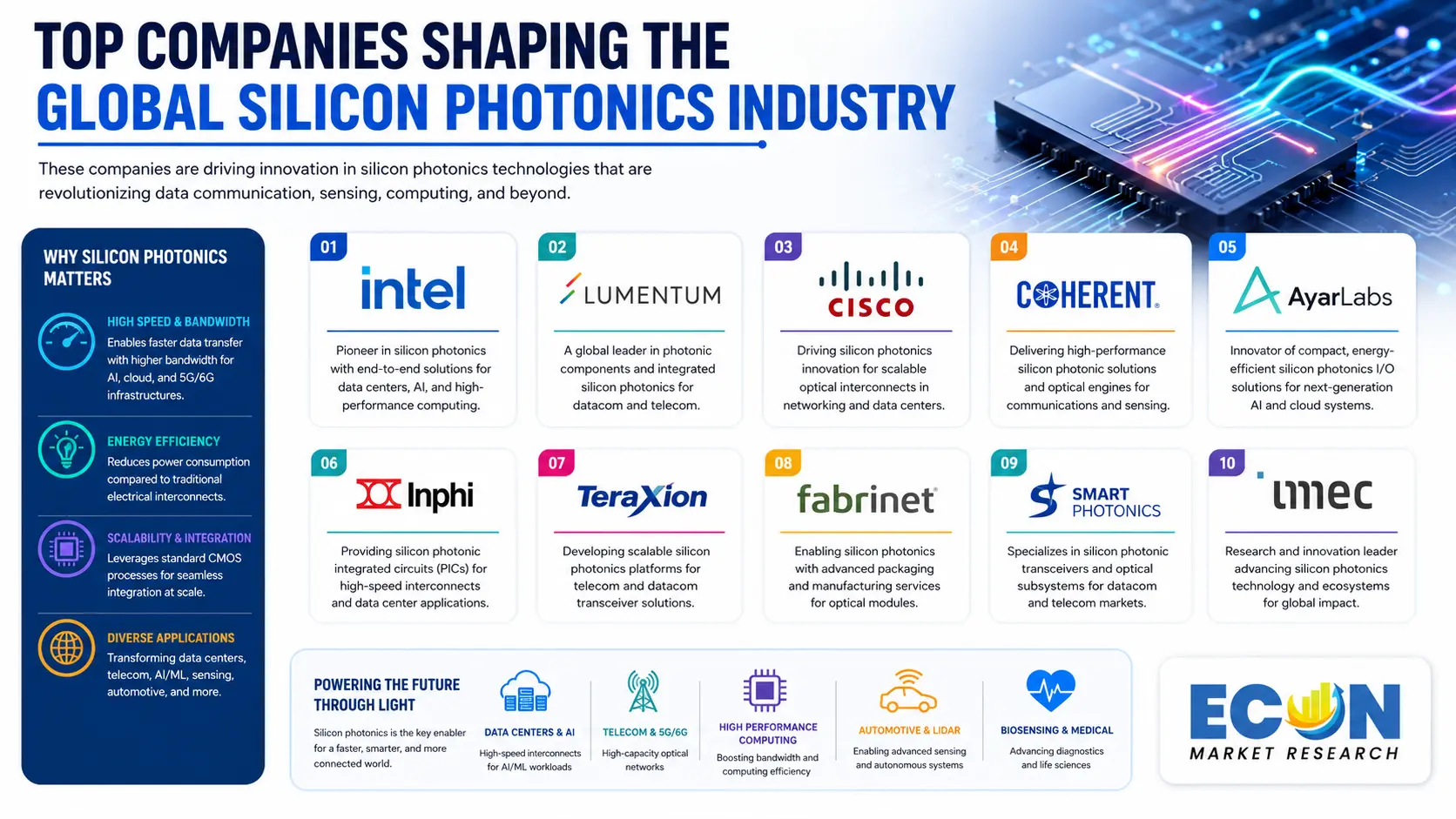
Top 10 Companies in the Silicon Photonics Industry
The following companies are presented without a strict ranking. Selection is based on silicon-photonics product capability, manufacturing scale, intellectual property, deployment history, foundry access, packaging expertise, optical-system integration, and relevance to AI, cloud, telecommunications, and high-performance computing applications.
1. Intel Corporation
Company Overview: Intel was founded in 1968 and is headquartered in Santa Clara, California, United States. Its silicon-photonics operations have supplied commercial data-center products since 2016, establishing a shipment base of 8 million-plus photonic integrated circuits and 32 million-plus integrated lasers. Core Silicon Photonics Expertise: Intel combines photonic integrated circuits, lasers, semiconductor optical amplifiers, modulators, detectors, electronic control circuitry, advanced packaging, and high-volume wafer processing. Its manufacturing record includes a laser failure-in-time rate below 0.1, which is important for hyperscale data centers where replacement rates and network downtime directly affect operating reliability. Major Products and Services: Intel supplies silicon-photonics components used in pluggable transceiver modules and has demonstrated a fully integrated 4-Tbps bidirectional optical compute-interconnect chiplet. The chiplet is designed for co-packaging with CPUs, GPUs, infrastructure processors, and other computing devices to support disaggregated architectures, memory pooling, and longer-reach optical links.
2. Cisco Systems, Inc.
Company Overview: Cisco was founded in 1984 and maintains its corporate headquarters in San Jose, California, United States. The company expanded its optical technology portfolio by completing the acquisition of Acacia Communications in March 2021. Acacia had selected silicon photonics as its coherent-integration platform in 2012, giving Cisco an established base in photonic integrated circuits, coherent digital signal processing, modules, and optical-network design. Core Silicon Photonics Expertise: Cisco develops networking silicon, switches, routers, transceivers, coherent optics, packaging, firmware, and network-management software within a vertically coordinated architecture. Major Products and Services: Its current silicon-photonics portfolio covers 400G, 800G, and 1.6T pluggable optics for AI front-end and back-end networks. Cisco’s 102.4-Tbps-class switching systems support configurations with 64 high-speed ports, enabling operators to combine photonic modules with Silicon One switching platforms and validated network designs.
3. NVIDIA Corporation
Company Overview: NVIDIA was founded in 1993 and is headquartered in Santa Clara, California, United States. The company entered silicon-photonics networking at system level by integrating photonic engines with its Spectrum-X Ethernet and Quantum-X InfiniBand switching platforms. Core Silicon Photonics Expertise: NVIDIA’s strength lies in coordinating graphics processors, AI accelerators, networking silicon, switching systems, software, photonic engines, external lasers, connectors, packaging, and data-center reference architectures. Major Products and Services: Its co-packaged photonics platforms support 1.6 Tbps per port and are designed for AI factories containing up to millions of GPUs. NVIDIA reports 3.5 times greater power efficiency, 10 times improved network resilience, 63 times stronger signal integrity, and 1.3 times faster deployment compared with traditional networking approaches. The company is working with semiconductor, laser, fiber, connector, and manufacturing partners to develop an integrated supply chain rather than treating silicon photonics as an isolated component technology.
4. Broadcom Inc.
Company Overview: Broadcom is headquartered in San Jose, California, and began its focused investment in highly integrated silicon photonics and co-packaged optics in 2019. Its role in the industry combines high-capacity switch silicon with optical engines, digital signal processors, transimpedance amplifiers, drivers, packaging, fiber attachment, and system-level reference designs. Core Silicon Photonics Expertise: Broadcom’s Silicon Photonics Chiplets in Package platform places photonic engines beside Ethernet-switch application-specific integrated circuits to reduce electrical link length and optical-connectivity power. Major Products and Services: The 51.2-Tbps Bailly platform integrates 8 optical engines rated at 6.4 Tbps each with a Tomahawk 5 switch chip. Broadcom introduced third-generation CPO technology supporting 200 Gbps per lane in May 2025 and disclosed development of a fourth-generation 400-Gbps-per-lane platform. Its 400G DR4+ pluggable transceiver also supports transmission across 2 kilometers of single-mode fiber.
5. Marvell Technology, Inc.
Company Overview: Marvell was founded in 1995 and is headquartered in Santa Clara, California, United States. Its silicon-photonics technology has accumulated 10 billion-plus device hours in hyperscale deployments and has been shipping commercially for 8 years-plus. Core Silicon Photonics Expertise: Marvell combines optical digital signal processors, transimpedance amplifiers, drivers, retimers, switch silicon, custom accelerators, photonic integrated circuits, firmware, and advanced packaging. The company’s strategy covers pluggable modules, linear-drive optics, on-board optics, co-packaged switches, and optical connectivity for custom AI accelerators. Major Products and Services: Its 1.6T light engine supports 200 Gbps per lane and integrates the photonic chip, driver, receiver electronics, controller, and firmware in one package. Marvell has also demonstrated a 6.4T light engine for co-packaged optics and an accelerator architecture intended to expand AI scale-up domains from tens of processors inside one rack to hundreds across multiple racks.
6. GlobalFoundries Inc.
Company Overview: GlobalFoundries was formed in 2009 and has maintained its global headquarters at its Malta, New York, manufacturing site since 2021. The company operates semiconductor manufacturing facilities across the United States, Europe, and Asia. Core Silicon Photonics Expertise: Its GF Fotonix platform combines photonics, 300-GHz-class radio-frequency CMOS, and digital logic on a 300-mm wafer. The platform supports 200 Gbps per wavelength, a development path toward 400 Gbps per wavelength, and bidirectional dense wavelength-division multiplexing with 8 or 16 wavelengths. Major Products and Services: GlobalFoundries provides foundry fabrication, process-design kits, design flows, multi-project wafer access, packaging support, fiber-attachment partnerships, and turnkey manufacturing. Its SCALE solution, introduced in May 2026, supports the Optical Compute Interconnect Multi-Source Agreement and uses both coarse and dense wavelength multiplexing for AI scale-up systems.
7. Tower Semiconductor Ltd.
Company Overview: Tower Semiconductor was founded in 1993 through the acquisition of a 150-mm wafer facility and is headquartered in Migdal Haemek, Israel. The company reports 7 manufacturing facilities, a global design center in Netanya, and a workforce of 5,500 employees including its Japanese operations. Core Silicon Photonics Expertise: Tower provides specialty-foundry platforms for silicon photonics, silicon-germanium BiCMOS, mixed-signal electronics, radio-frequency devices, image sensors, and 3D wafer integration. Its PH18 silicon-photonics platform supports high-volume datacom, telecom, sensing, and AI applications. Major Products and Services: Tower and OpenLight demonstrated a 400-Gbps-per-lane modulator using PAM-4 signaling, a 0.6-volt peak-to-peak drive, and an extinction ratio above 3.5 dB. Tower also supports production at 100 Gbps and 200 Gbps per lane and introduced wafer-scale 3D integration for co-packaging photonic and electronic processes in 2025.
8. Coherent Corp.
Company Overview: Coherent was founded in 1971, is headquartered in Saxonburg, Pennsylvania, United States, and operates in 20-plus countries. Its vertically integrated portfolio covers engineered materials, lasers, photonic integrated circuits, optical components, transceivers, amplifiers, optical circuit switches, and semiconductor-manufacturing technologies. Core Silicon Photonics Expertise: Coherent can combine silicon-photonics circuits with internally supplied continuous-wave lasers, photodetectors, passive components, optical packaging, digital signal processors, and fiber-management technologies. Major Products and Services: The company demonstrated a 1.6T-DR8 silicon-photonics module with 200-Gbps electrical and optical interfaces and a 3-nm digital signal processor intended to reduce transceiver power by 20%. Its 2x400G-FR4 Lite module provides a 500-meter reach and eliminates the thermoelectric cooler, while its broader roadmap includes 3.2T and 12.8T connectivity technologies.
9. Ayar Labs, Inc.
Company Overview: Ayar Labs was founded in 2015 and is headquartered in San Jose, California, United States. The company originated from academic work on replacing electrical serializer-deserializer interfaces with optical chiplets for direct processor connectivity. Core Silicon Photonics Expertise: Ayar Labs focuses on in-package optical I/O, multi-wavelength light sources, chiplet interfaces, fiber coupling, thermal control, and scale-up architectures for AI and high-performance computing. Major Products and Services: Its TeraPHY optical chiplet supports 8 Tbps of bandwidth and connects to a 16-wavelength SuperNova light source. The 2025 generation introduced a UCIe electrical interface to simplify integration with accelerators from different vendors. Engineering tests subjected the chiplet to temperature-change rates reaching 800°C per second while maintaining bit-error performance within specification. Ayar Labs also works with ASIC designers, foundries, packaging companies, system manufacturers, and aerospace suppliers to move optical I/O from demonstrations into deployable systems.
10. Lightmatter, Inc.
Company Overview: Lightmatter was founded by Massachusetts Institute of Technology researchers in 2017 and is headquartered in Mountain View, California, United States. The company develops photonic interconnect platforms that place optical routing beneath or beside processors rather than restricting high-bandwidth interfaces to the chip perimeter. Core Silicon Photonics Expertise: Lightmatter specializes in active photonic interposers, 3D co-packaged optics, optical switching, wavelength routing, chip-to-chip connectivity, and packaging architectures for large AI systems. Major Products and Services: Passage L200 is available in 32-Tbps and 64-Tbps configurations and is designed to deliver 200-Tbps-plus total package I/O. The Passage M1000 reference platform measures 4,000 square millimeters and supplies 114 Tbps of aggregate optical bandwidth. Lightmatter states that its architecture can support thousands of GPUs within one connectivity domain and reduce advanced-model training time by up to 8 times by removing processor-to-processor bandwidth constraints.
Regional Outlook
North America
North America has the most concentrated commercial silicon-photonics ecosystem because the United States hosts Intel, Cisco, NVIDIA, Broadcom, Marvell, GlobalFoundries, Coherent, Ayar Labs, and Lightmatter. The region’s strongest demand originates from hyperscale cloud facilities, AI computing clusters, telecommunications operators, defense systems, semiconductor research laboratories, and optical-network manufacturers. AIM Photonics, established in 2015, gives companies and universities access to 300-mm silicon and silicon-nitride processes, multi-project wafers, packaging, testing, and design tools. Its Test, Assembly and Packaging facility provides submicrometer placement capability with tolerances reaching 0.5 micrometers, addressing one of the most difficult stages in photonic manufacturing.
The United States also has an expanding domestic production base in New York, Pennsylvania, California, Arizona, and other semiconductor clusters. GlobalFoundries manufactures GF Fotonix technology in Malta, while AIM Photonics fabricates 300-mm photonic devices in Albany. Canada contributes through silicon-photonics design, photonic wire bonding, quantum technologies, telecommunications research, and National Research Council programs covering silicon photonics and advanced detectors. SiEPICfab expanded Canadian fabrication and packaging capabilities in 2025, while Canadian researchers continue developing inverse-designed filters, metamaterial circuits, and AI-assisted photonic fabrication. Mexico has a less-developed photonic-wafer ecosystem but participates in electronics assembly, automotive sensing, telecommunications deployment, and North American manufacturing supply chains. The principal regional challenge is coordinating optical design, wafer fabrication, laser supply, packaging, fiber attachment, testing, and skilled labor within one scalable production network.
Europe
Europe combines established photonics research with specialized semiconductor manufacturing in Belgium, France, Germany, the Netherlands, Spain, Italy, Ireland, Finland, and the United Kingdom. The European Chips Act launched 5 semiconductor pilot lines covering sub-2-nm logic, fully depleted silicon-on-insulator technology, advanced packaging, wide-bandgap materials, and photonic integrated circuits. By May 2026, the photonic pilot line provided open-access services through 14 hosting sites across silicon, silicon nitride, indium phosphide, packaging, testing, and reliability platforms. This distributed structure helps European start-ups and small manufacturers access fabrication capabilities that would be impractical to build independently.
The PIXEurope program began in June 2025 and is scheduled to run until May 2030, creating a coordinated route from design and prototyping to pilot-scale photonic production. Belgium’s imec contributes advanced semiconductor processes and packaging; France’s CEA-Leti supports silicon-on-insulator and heterogeneous integration; the Netherlands has strong photonics design and quantum capabilities; and Spain coordinates open-access integrated-photonics activity. Germany and Italy provide materials, equipment, automotive electronics, sensing, and specialty manufacturing expertise. Europe’s opportunity lies in industrial, automotive, healthcare, quantum, sensing, and energy-efficient data-center applications rather than relying entirely on hyperscale networking. Challenges include fragmented national programs, limited high-volume optical packaging, shortages of cross-disciplinary engineers, and the need to translate laboratory devices into qualified products with 10-year or 20-year operating lifetimes.
Asia-Pacific
Asia-Pacific is central to silicon-photonics manufacturing because Taiwan, Singapore, Japan, South Korea, and China possess extensive semiconductor foundry, packaging, substrate, laser, connector, optical-module, and electronics-assembly capacity. Singapore began its national silicon-photonics research program in 2007, formed the Lux Photonics Consortium in 2015, and supported the creation of Advanced Micro Foundry in 2017. The country manufactures 1 in 10 chips and 1 in 5 semiconductor-equipment units globally, while its semiconductor workforce includes 35,000-plus employees. Singapore has identified silicon photonics and advanced packaging as strategic technologies for AI infrastructure and established shared facilities for prototyping and small-volume manufacturing.
Taiwan’s ecosystem connects advanced wafer fabrication, ASIC design, packaging, optical modules, and server manufacturing, making it essential for co-packaged optics and optical I/O. Japan contributes high-purity materials, lasers, sensors, manufacturing equipment, fiber, and photonic-component expertise, while government programs support next-generation semiconductor and photonics collaboration. South Korea’s memory and advanced-packaging industries create opportunities for optical links between accelerators and high-bandwidth memory. India is building research capability through institutions such as IIT Madras, where a government-supported silicon-photonics center issued an industry-participation call in February 2026. Australia contributes quantum photonics and university research, while Southeast Asian economies support electronics assembly and testing. Regional risks include export restrictions, geographic concentration, intellectual-property protection, supply-chain disruptions, and dependence on a limited number of advanced foundries and packaging providers.
Middle East & Africa
The Middle East and Africa have smaller commercial silicon-photonics manufacturing bases, but Israel, Saudi Arabia, the United Arab Emirates, and South Africa possess relevant capabilities in semiconductors, photonics, lasers, defense, sensing, communications, and artificial intelligence. Israel combines Tower Semiconductor’s foundry operations with start-ups, university laboratories, optical-network companies, and defense-electronics manufacturers. In 2025, Israel joined a 9-country international initiative focused on resilient AI and semiconductor supply chains. Saudi Arabia’s KAUST published research on CMOS-integrated silicon photonics, hybrid lasers, optical-comb sources, and links approaching sub-picojoule-per-bit energy consumption, creating a research base for data-center, sensing, and quantum applications.
South Africa operates a Photonics Prototyping Facility at the Council for Scientific and Industrial Research. The facility includes Class 1,000 cleanrooms and supports prototype development for communications, healthcare, manufacturing, mining, energy, security, and sensing. The United Arab Emirates and Qatar are potential deployment markets because their data-center, cloud, telecommunications, and AI programs require high-bandwidth optical networks, even though local photonic-wafer manufacturing remains limited. Egypt, Kenya, and Nigeria can participate through fiber-network expansion, university research, electronics integration, and regional data centers. The principal barriers are limited access to semiconductor fabs, shortages of photonic-design and packaging engineers, dependence on imported lasers and wafers, insufficient testing infrastructure, and low production volumes. Regional progress is therefore likely to begin with research, design, system integration, specialized sensing, and optical-network deployment before full wafer-scale manufacturing.
Future Opportunities in the Silicon Photonics Industry
The strongest future opportunity is the movement of optical connectivity from the network edge into processor packages. Current systems use 1.6T modules and 200-Gbps lanes, while development programs are already demonstrating 400-Gbps-per-lane modulators, 3.2T transceivers, 64-Tbps photonic engines, and 114-Tbps optical interposers. This progression could enable accelerators, memory, storage, and switching components to communicate across multiple racks without the reach and power penalties of high-speed copper. Verified development targets include Broadcom’s fourth-generation 400-Gbps-per-lane CPO platform, Tower Semiconductor’s 3.2T-oriented modulator, and Coherent’s work on 3.2T and 12.8T connectivity. Analytical expectations should remain conditional because deployment will depend on reliability, repairability, laser architecture, connector standards, thermal design, manufacturing yield, and customer qualification.
Additional opportunities include autonomous-vehicle LiDAR, medical imaging, biosensing, microwave photonics, quantum computing, precision timing, telecommunications access networks, and industrial inspection. GlobalFoundries’ 16-wavelength bidirectional platform illustrates how dense wavelength multiplexing can increase bandwidth without adding equal numbers of fibers. NIST has demonstrated silicon-nitride devices on 300-mm wafers, indicating that silicon photonics can expand into frequency combs, atomic references, spectroscopy, and navigation systems. Artificial intelligence can also improve photonic design through inverse optimization, process correction, automated layout, and predictive yield analysis. Workforce development will be decisive because commercial products require engineers who understand optics, semiconductor processing, radio-frequency electronics, packaging, thermal control, firmware, and network architecture. Open-access foundries and pilot lines can reduce entry barriers for start-ups and small manufacturers, but standardized testing and interoperable chiplet interfaces must mature before optical I/O becomes a default computing technology.
Conclusion
The silicon photonics industry has entered a commercial transition defined by 1.6T transceivers, 200-Gbps optical lanes, 51.2-Tbps and 102.4-Tbps switches, co-packaged optics, wavelength-multiplexed light sources, and optical I/O chiplets. The 5 central trends—CPO commercialization, 1.6T and 3.2T connectivity, UCIe optical chiplets, integrated light sources, and industrialized packaging—are moving photonics closer to processors and switching silicon. Intel’s 8 million-plus PIC shipments demonstrate established production scale, while newer platforms from NVIDIA, Broadcom, Marvell, Ayar Labs, and Lightmatter illustrate the shift toward optical connectivity for large AI systems. Foundries and manufacturing specialists such as GlobalFoundries and Tower Semiconductor provide the process infrastructure needed to convert these architectures into repeatable products.
The Top Companies in the Silicon Photonics Industry represent different parts of one interconnected value chain rather than a simple ranking. North America leads in AI-system architecture, networking silicon, and optical chiplets; Europe maintains strong pilot-line, research, automotive, sensing, and quantum capabilities; Asia-Pacific provides extensive foundry, packaging, laser, module, and electronics-manufacturing capacity; and the Middle East and Africa are building research, sensing, defense, and deployment capabilities. Future competitiveness will depend on 300-mm manufacturing, submicrometer packaging accuracy, 400-Gbps-per-lane development, standardized chiplet interfaces, lower energy per bit, automated testing, and resilient laser supply. Companies that coordinate photonic design, electronics, packaging, software, reliability, and manufacturing will be positioned to support the next generation of AI, cloud, telecommunications, sensing, and high-performance computing infrastructure.